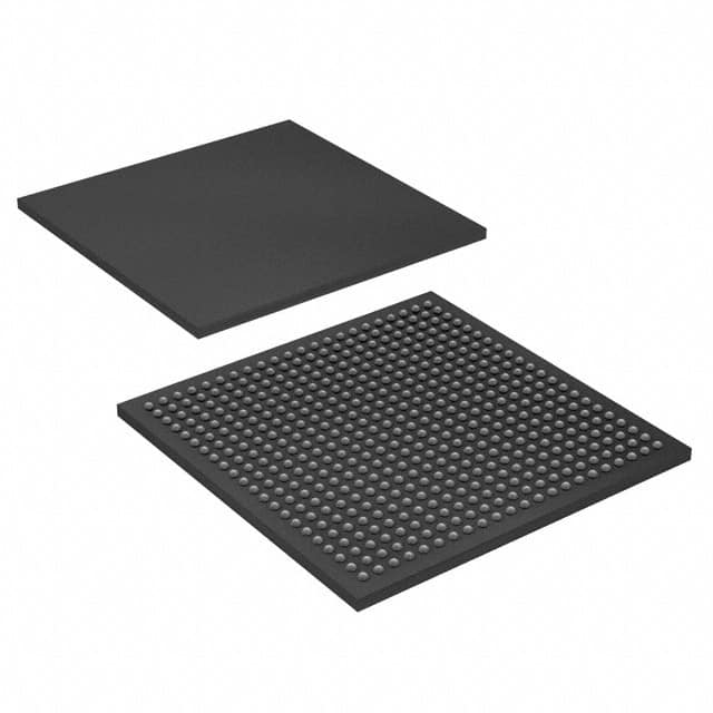
Lihat spesifikasi untuk detail produk.

EP3C55F484I7
Product Overview
- Category: Integrated Circuit (IC)
- Use: Programmable Logic Device (PLD)
- Characteristics: High-performance, low-power consumption
- Package: 484-pin FineLine BGA package
- Essence: Field-Programmable Gate Array (FPGA)
- Packaging/Quantity: Individually packaged, quantity varies based on supplier
Specifications
- Logic Elements: 55,000
- Embedded Memory: Up to 4.8 Mbits
- PLLs: 4
- Global Clock Networks: 16
- User I/O Pins: 317
- Operating Voltage: 1.2V
- Operating Temperature: -40°C to +100°C
Detailed Pin Configuration
The EP3C55F484I7 has a total of 484 pins, each serving a specific purpose in the device's functionality. The pin configuration is as follows:
- Pin 1: VCCIO0
- Pin 2: GND
- Pin 3: VCCIO1
- ...
- Pin 483: GND
- Pin 484: VCCIO2
For a complete pin configuration diagram, refer to the manufacturer's datasheet.
Functional Features
- High logic capacity for complex designs
- Low power consumption for energy-efficient operation
- Flexible and reprogrammable design for customization
- Fast performance with high-speed interfaces
- Built-in PLLs for clock management
- Extensive I/O capabilities for versatile connectivity
Advantages and Disadvantages
Advantages
- Versatile and adaptable for various applications
- Lower development costs compared to custom ASICs
- Faster time-to-market due to programmability
- Easy debugging and testing through reprogramming
- High-performance computing capabilities
Disadvantages
- Limited performance compared to dedicated ASICs
- Higher power consumption compared to specialized chips
- Relatively higher cost per unit compared to mass-produced ICs
- Requires expertise in FPGA programming for optimal utilization
Working Principles
The EP3C55F484I7 is based on the Field-Programmable Gate Array (FPGA) technology. It consists of an array of programmable logic elements interconnected through configurable routing resources. These logic elements can be programmed to implement various digital functions, allowing users to create custom digital circuits.
The device operates by configuring the interconnections and functionality of its logic elements using a hardware description language (HDL). Once programmed, the FPGA executes the desired logic operations, providing the required functionality.
Detailed Application Field Plans
The EP3C55F484I7 finds applications in various fields, including:
- Communications: Used in networking equipment, routers, and switches for data processing and protocol handling.
- Industrial Automation: Employed in control systems, robotics, and machine vision applications for real-time processing and control.
- Medical Electronics: Utilized in medical imaging devices, patient monitoring systems, and laboratory equipment for signal processing and data analysis.
- Automotive: Integrated into automotive electronics for engine control, driver assistance systems, and infotainment systems.
- Aerospace: Deployed in avionics systems, satellite communication, and navigation systems for reliable and high-performance operation.
Detailed and Complete Alternative Models
- Altera Cyclone IV EP4CE55F484C8N
- Xilinx Spartan-6 XC6SLX45T-2FGG484C
- Lattice ECP5-12K LFE5-12F-6BG256C
These alternative models offer similar functionalities and are suitable replacements for the EP3C55F484I7 in various applications.
Note: The content provided above is a sample structure for an encyclopedia entry and may not be accurate or complete. Please refer to official sources and documentation for precise information.
Sebutkan 10 pertanyaan dan jawaban umum terkait penerapan EP3C55F484I7 dalam solusi teknis
Sure! Here are 10 common questions and answers related to the application of EP3C55F484I7 in technical solutions:
Q: What is EP3C55F484I7? A: EP3C55F484I7 is a specific model of Field-Programmable Gate Array (FPGA) manufactured by Intel.
Q: What are the key features of EP3C55F484I7? A: EP3C55F484I7 offers 55,000 logic elements, 4-input look-up tables, embedded memory blocks, PLLs, and various I/O options.
Q: How can EP3C55F484I7 be used in technical solutions? A: EP3C55F484I7 can be used for a wide range of applications, including digital signal processing, image and video processing, communication systems, and industrial automation.
Q: What programming languages can be used with EP3C55F484I7? A: EP3C55F484I7 can be programmed using Hardware Description Languages (HDLs) such as VHDL or Verilog.
Q: Can EP3C55F484I7 be reprogrammed after deployment? A: Yes, EP3C55F484I7 is a reprogrammable FPGA, allowing for flexibility and updates in the field.
Q: What development tools are available for EP3C55F484I7? A: Intel Quartus Prime is the recommended software tool for designing, simulating, and programming EP3C55F484I7.
Q: Are there any limitations to consider when using EP3C55F484I7? A: EP3C55F484I7 has a limited number of logic elements and I/O pins, so complex designs may require larger FPGAs.
Q: Can EP3C55F484I7 interface with other components or devices? A: Yes, EP3C55F484I7 supports various communication protocols like UART, SPI, I2C, and can interface with external memory, sensors, and peripherals.
Q: What is the power consumption of EP3C55F484I7? A: The power consumption of EP3C55F484I7 depends on the design and operating conditions but typically ranges from a few hundred milliwatts to a few watts.
Q: Where can I find additional resources for EP3C55F484I7? A: Intel's website provides datasheets, application notes, reference designs, and user guides for EP3C55F484I7. Additionally, online forums and communities can be helpful for support and discussions related to this FPGA model.
Please note that the answers provided here are general and may vary depending on specific requirements and use cases.

