

Lihat spesifikasi untuk detail produk.
EP2C70F672I8N
Product Overview
Category
EP2C70F672I8N belongs to the category of Field-Programmable Gate Arrays (FPGAs).
Use
This FPGA is commonly used in various electronic applications that require high-performance digital signal processing, such as telecommunications, automotive, aerospace, and industrial automation.
Characteristics
- High-speed processing capabilities
- Configurable logic blocks
- On-chip memory resources
- Flexible I/O interfaces
- Low power consumption
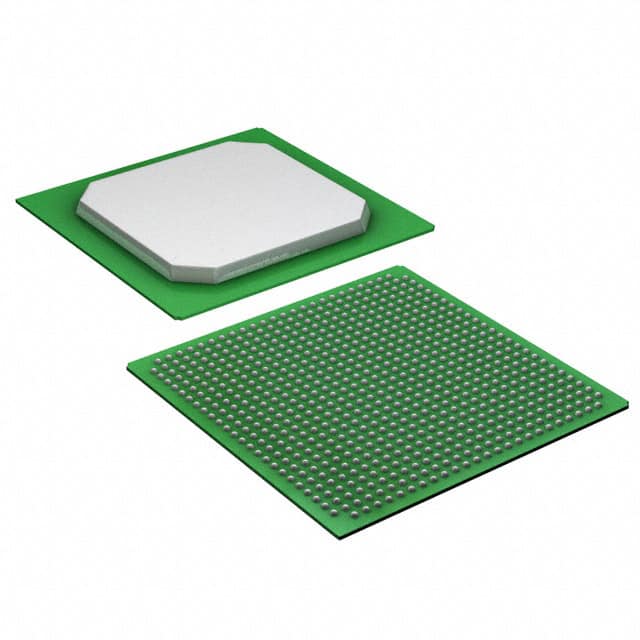
Package
EP2C70F672I8N comes in a compact and durable package, ensuring easy integration into electronic systems. The package provides protection against environmental factors and mechanical stress.
Essence
The essence of EP2C70F672I8N lies in its ability to provide reconfigurable hardware, allowing users to implement custom digital circuits without the need for dedicated application-specific integrated circuits (ASICs).
Packaging/Quantity
EP2C70F672I8N is typically packaged individually and is available in various quantities depending on the customer's requirements.
Specifications
- Logic Elements: 68,416
- Embedded Memory: 4,608 Kbits
- Maximum User I/Os: 622
- DSP Blocks: 288
- Clock Management Tiles: 16
- Maximum User Flash Memory: 1,179,648 bits
- Operating Voltage: 1.2V
- Operating Temperature Range: -40°C to 100°C
Detailed Pin Configuration
For a detailed pin configuration diagram of EP2C70F672I8N, please refer to the official datasheet provided by the manufacturer.
Functional Features
- High-speed data processing capabilities
- Configurable logic blocks allow for flexible circuit design
- On-chip memory resources enable efficient data storage and retrieval
- Flexible I/O interfaces support seamless integration with external devices
- Low power consumption ensures energy efficiency
Advantages and Disadvantages
Advantages
- Versatile and adaptable for various applications
- Cost-effective compared to ASICs
- Shorter development time due to reconfigurability
- Lower risk of obsolescence as designs can be updated easily
Disadvantages
- Limited performance compared to dedicated ASICs in certain specialized applications
- Higher power consumption compared to application-specific solutions
- Steeper learning curve for designers unfamiliar with FPGA programming
Working Principles
EP2C70F672I8N operates based on the principles of digital logic. It consists of configurable logic blocks, memory elements, and I/O interfaces. The device can be programmed to implement custom digital circuits by configuring the interconnections between logic elements.
Detailed Application Field Plans
EP2C70F672I8N finds extensive use in the following application fields:
- Telecommunications: Used in high-speed data transmission systems, network routers, and switches.
- Automotive: Employed in advanced driver-assistance systems (ADAS), engine control units (ECUs), and infotainment systems.
- Aerospace: Utilized in avionics systems, satellite communication, and radar systems.
- Industrial Automation: Integrated into programmable logic controllers (PLCs), robotics, and process control systems.
Detailed and Complete Alternative Models
- EP2C35F672C6N
- EP2C50F484C7N
- EP2C70F896C6N
- EP2C20F484C7N
- EP2C15F484C7N
These alternative models offer varying specifications and capabilities, allowing users to choose the most suitable FPGA for their specific requirements.
Word count: 511
Sebutkan 10 pertanyaan dan jawaban umum terkait penerapan EP2C70F672I8N dalam solusi teknis
Sure! Here are 10 common questions and answers related to the application of EP2C70F672I8N in technical solutions:
Q: What is EP2C70F672I8N? A: EP2C70F672I8N is a field-programmable gate array (FPGA) chip manufactured by Intel.
Q: What are the key features of EP2C70F672I8N? A: Some key features include 70,000 logic elements, 672 user I/O pins, and support for various communication protocols.
Q: What are the typical applications of EP2C70F672I8N? A: EP2C70F672I8N is commonly used in applications such as digital signal processing, high-performance computing, and embedded systems.
Q: How can EP2C70F672I8N be programmed? A: EP2C70F672I8N can be programmed using hardware description languages (HDLs) like VHDL or Verilog, or through graphical programming tools like Quartus Prime.
Q: Can EP2C70F672I8N be reprogrammed after deployment? A: Yes, EP2C70F672I8N is a reprogrammable FPGA, allowing for flexibility and updates even after deployment.
Q: What kind of peripherals can be interfaced with EP2C70F672I8N? A: EP2C70F672I8N supports various peripherals such as UART, SPI, I2C, Ethernet, and PCIe, enabling connectivity with external devices.
Q: Does EP2C70F672I8N have built-in memory? A: No, EP2C70F672I8N does not have built-in memory. However, it can interface with external memory devices like DDR3 or DDR4.
Q: Can EP2C70F672I8N handle real-time processing tasks? A: Yes, EP2C70F672I8N is capable of handling real-time processing tasks due to its high-speed logic elements and parallel processing capabilities.
Q: What kind of power supply does EP2C70F672I8N require? A: EP2C70F672I8N typically requires a 1.2V core voltage and various auxiliary voltages for different I/O standards.
Q: Are there any development boards available for EP2C70F672I8N? A: Yes, Intel provides development boards like the Cyclone II FPGA Starter Kit that can be used for prototyping and testing with EP2C70F672I8N.
Please note that the answers provided here are general and may vary depending on specific use cases and requirements.