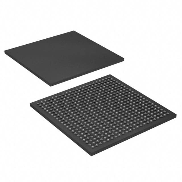
Lihat spesifikasi untuk detail produk.

EP2C35F484C8
Product Overview
- Category: Integrated Circuit (IC)
- Use: Programmable Logic Device (PLD)
- Characteristics: High-performance, low-power consumption
- Package: 484-pin FineLine BGA (Ball Grid Array)
- Essence: Field-Programmable Gate Array (FPGA)
- Packaging/Quantity: Single unit per package
Specifications
- Logic Elements: 33,216
- RAM Bits: 1,152 Kbits
- Embedded Multipliers: 66
- Maximum User I/Os: 317
- Operating Voltage: 1.2V
- Speed Grade: C8 (Commercial Grade 8)
Detailed Pin Configuration
The EP2C35F484C8 has a total of 484 pins, each serving a specific purpose in the device's functionality. The pin configuration includes power supply pins, ground pins, configuration pins, input/output pins, and specialized pins for various functions.
For a detailed pin configuration diagram, please refer to the manufacturer's datasheet.
Functional Features
- High Performance: The EP2C35F484C8 offers a large number of logic elements and embedded multipliers, enabling high-speed processing and complex computations.
- Low Power Consumption: With its advanced architecture and optimized power management techniques, this PLD minimizes power consumption, making it suitable for battery-powered applications.
- Flexibility: Being a field-programmable device, it allows users to configure and reconfigure the logic functions according to their specific requirements.
- Versatility: The FPGA can be used for a wide range of applications, including digital signal processing, data encryption, and control systems.
Advantages and Disadvantages
Advantages: - High performance and flexibility due to programmability - Low power consumption - Suitable for a variety of applications
Disadvantages: - Relatively complex programming process - Higher cost compared to fixed-function integrated circuits
Working Principles
The EP2C35F484C8 is based on the concept of a Field-Programmable Gate Array (FPGA). It consists of an array of configurable logic blocks interconnected through programmable interconnects. The device can be programmed using Hardware Description Languages (HDL) such as VHDL or Verilog, which define the desired logic functions and interconnections.
Once programmed, the FPGA executes the specified logic operations, allowing for the implementation of complex digital systems.
Detailed Application Field Plans
The EP2C35F484C8 finds applications in various fields, including:
- Communications: Used in wireless base stations, network routers, and data transmission equipment.
- Industrial Automation: Employed in control systems, robotics, and factory automation.
- Aerospace and Defense: Utilized in radar systems, avionics, and military communication devices.
- Medical Equipment: Integrated into medical imaging devices, patient monitoring systems, and diagnostic instruments.
- Consumer Electronics: Found in high-definition televisions, gaming consoles, and multimedia devices.
Detailed and Complete Alternative Models
- EP2C20F484C8: A lower-density version of the EP2C35F484C8 with 20,352 logic elements.
- EP2C70F484C8: A higher-density version of the EP2C35F484C8 with 68,416 logic elements.
- EP4CE115F29C8N: An alternative FPGA from a different manufacturer, offering similar capabilities with 115,200 logic elements.
These alternative models provide options with varying logic densities to suit different project requirements.
Word count: 346 words
Sebutkan 10 pertanyaan dan jawaban umum terkait penerapan EP2C35F484C8 dalam solusi teknis
Sure! Here are 10 common questions and answers related to the application of EP2C35F484C8 in technical solutions:
Q: What is EP2C35F484C8? A: EP2C35F484C8 is a specific model of Field-Programmable Gate Array (FPGA) manufactured by Intel.
Q: What are the key features of EP2C35F484C8? A: Some key features include 35,200 logic elements, 1,288 Kbits of embedded memory, 266 user I/O pins, and support for various communication protocols.
Q: What are the typical applications of EP2C35F484C8? A: EP2C35F484C8 is commonly used in applications such as digital signal processing, industrial automation, robotics, telecommunications, and high-performance computing.
Q: How can EP2C35F484C8 be programmed? A: EP2C35F484C8 can be programmed using Hardware Description Languages (HDLs) like VHDL or Verilog, which describe the desired functionality of the FPGA.
Q: Can EP2C35F484C8 be reprogrammed after initial programming? A: Yes, EP2C35F484C8 is a reprogrammable FPGA, allowing users to modify and update the design even after it has been initially programmed.
Q: What development tools are available for EP2C35F484C8? A: Intel provides Quartus Prime software suite, which includes tools for designing, simulating, and programming EP2C35F484C8 FPGAs.
Q: Does EP2C35F484C8 support external memory interfaces? A: Yes, EP2C35F484C8 supports various external memory interfaces such as DDR3, DDR4, and QDR II+.
Q: Can EP2C35F484C8 interface with other devices or peripherals? A: Yes, EP2C35F484C8 has multiple I/O pins that can be used to interface with other devices or peripherals like sensors, displays, or communication modules.
Q: What is the power consumption of EP2C35F484C8? A: The power consumption of EP2C35F484C8 depends on the specific design and operating conditions but typically ranges from a few watts to tens of watts.
Q: Are there any known limitations or considerations when using EP2C35F484C8? A: Some considerations include the need for proper cooling due to potential heat dissipation, careful power supply design, and understanding the timing constraints of the FPGA design.
Please note that these answers are general and may vary depending on the specific requirements and implementation of EP2C35F484C8 in a technical solution.

