

Lihat spesifikasi untuk detail produk.
EP2AGX65DF25C6NES
Product Overview
Category
EP2AGX65DF25C6NES belongs to the category of Field Programmable Gate Arrays (FPGAs).
Use
FPGAs are integrated circuits that can be programmed and reprogrammed to perform various digital functions. They are widely used in industries such as telecommunications, automotive, aerospace, and consumer electronics.
Characteristics
- EP2AGX65DF25C6NES is a high-performance FPGA designed for advanced applications.
- It offers a large number of logic elements, memory blocks, and high-speed transceivers.
- The device supports various I/O standards and has built-in security features.
- It operates at low power consumption levels while delivering high performance.
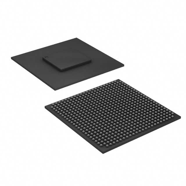
Package
EP2AGX65DF25C6NES comes in a compact package suitable for surface mount technology (SMT) assembly. The package ensures easy integration into electronic systems.
Essence
The essence of EP2AGX65DF25C6NES lies in its ability to provide flexible and customizable digital circuitry. Its programmability allows designers to implement complex functionalities without the need for custom-designed ASICs.
Packaging/Quantity
EP2AGX65DF25C6NES is typically packaged in trays or reels, depending on the quantity ordered. The packaging ensures safe transportation and handling during manufacturing and assembly processes.
Specifications
- Logic Elements: 65,536
- Memory Blocks: 2,048
- Transceivers: 24
- I/O Standards: LVCMOS, LVTTL, SSTL, HSTL, LVDS, RSDS, etc.
- Power Consumption: Low power operation with dynamic power management features
- Operating Temperature: -40°C to 100°C
- Supply Voltage: 1.2V
Detailed Pin Configuration
EP2AGX65DF25C6NES has a complex pin configuration with multiple I/O pins, power supply pins, and configuration pins. The detailed pin configuration can be found in the product datasheet provided by the manufacturer.
Functional Features
- High-performance FPGA with abundant logic elements and memory blocks.
- Support for various I/O standards enables easy interfacing with external devices.
- Built-in security features protect the design from unauthorized access or tampering.
- Dynamic power management allows efficient utilization of resources and reduces power consumption.
- The device offers high-speed transceivers for reliable data communication.
Advantages and Disadvantages
Advantages
- Flexibility: EP2AGX65DF25C6NES provides designers with the flexibility to implement custom digital circuits without the need for ASIC development.
- Reconfigurability: The FPGA can be reprogrammed multiple times, allowing for iterative design improvements and adaptability to changing requirements.
- High Performance: With a large number of logic elements and memory blocks, EP2AGX65DF25C6NES can handle complex applications efficiently.
- Integration: The compact package and support for various I/O standards facilitate seamless integration into electronic systems.
Disadvantages
- Complexity: Working with FPGAs requires specialized knowledge and expertise in digital design and programming.
- Cost: FPGAs can be more expensive compared to off-the-shelf microcontrollers or application-specific integrated circuits (ASICs) for certain applications.
- Power Consumption: While efforts have been made to reduce power consumption, FPGAs still consume more power compared to dedicated hardware solutions.
Working Principles
EP2AGX65DF25C6NES operates based on the principles of configurable logic. The FPGA consists of an array of programmable logic elements interconnected through configurable routing resources. These logic elements can be programmed to perform specific functions using a hardware description language (HDL) such as VHDL or Verilog. The configuration data is stored in internal memory blocks and can be loaded during startup or reprogrammed as needed.
Detailed Application Field Plans
EP2AGX65DF25C6NES finds applications in various fields, including:
- Telecommunications: Used in base stations, routers, and network switches for high-speed data processing and protocol handling.
- Automotive: Employed in advanced driver-assistance systems (ADAS), infotainment systems, and engine control units (ECUs) for real-time processing and control.
- Aerospace: Utilized in satellite communication systems, avionics, and radar systems for signal processing and data handling.
- Consumer Electronics: Integrated into smart TVs, gaming consoles, and wearable devices for multimedia processing and user interface control.
Detailed and Complete Alternative Models
- EP2AGX125EF35I5N
- EP4CE115F29C7N
- XC7A100T-1FGG484C
- LFE5UM5G-85F-8BG756I
These alternative models offer similar functionality and performance to EP2AGX
Sebutkan 10 pertanyaan dan jawaban umum terkait penerapan EP2AGX65DF25C6NES dalam solusi teknis
Sure! Here are 10 common questions and answers related to the application of EP2AGX65DF25C6NES in technical solutions:
Q: What is EP2AGX65DF25C6NES? A: EP2AGX65DF25C6NES is a specific model of field-programmable gate array (FPGA) manufactured by Intel.
Q: What are the key features of EP2AGX65DF25C6NES? A: Some key features include 65,536 logic elements, 2,048 embedded memory blocks, 4-phase locked loops (PLLs), and support for various I/O standards.
Q: What are the typical applications of EP2AGX65DF25C6NES? A: EP2AGX65DF25C6NES is commonly used in applications such as high-performance computing, telecommunications, industrial automation, and video processing.
Q: How can EP2AGX65DF25C6NES be programmed? A: EP2AGX65DF25C6NES can be programmed using hardware description languages (HDLs) like VHDL or Verilog, or through graphical programming tools like Quartus Prime.
Q: Can EP2AGX65DF25C6NES be reprogrammed after deployment? A: Yes, EP2AGX65DF25C6NES is a reprogrammable FPGA, allowing for flexibility and updates even after it has been deployed in a system.
Q: What are the power requirements for EP2AGX65DF25C6NES? A: The power requirements vary depending on the specific implementation, but typically range from 1.2V to 3.3V for core voltage and 1.8V to 3.3V for I/O voltage.
Q: Does EP2AGX65DF25C6NES support high-speed interfaces? A: Yes, EP2AGX65DF25C6NES supports various high-speed interfaces such as PCIe, DDR3/4 memory interfaces, Gigabit Ethernet, and USB.
Q: Can EP2AGX65DF25C6NES interface with other components or microcontrollers? A: Yes, EP2AGX65DF25C6NES can interface with other components or microcontrollers through its GPIO pins, serial communication protocols, or dedicated interfaces like I2C or SPI.
Q: Are there any development kits available for EP2AGX65DF25C6NES? A: Yes, Intel provides development kits that include the necessary hardware and software tools to get started with EP2AGX65DF25C6NES-based designs.
Q: What kind of technical support is available for EP2AGX65DF25C6NES? A: Intel offers technical documentation, online forums, and direct customer support to assist with any questions or issues related to EP2AGX65DF25C6NES.
Please note that the specific details and answers may vary based on the manufacturer's documentation and product specifications.