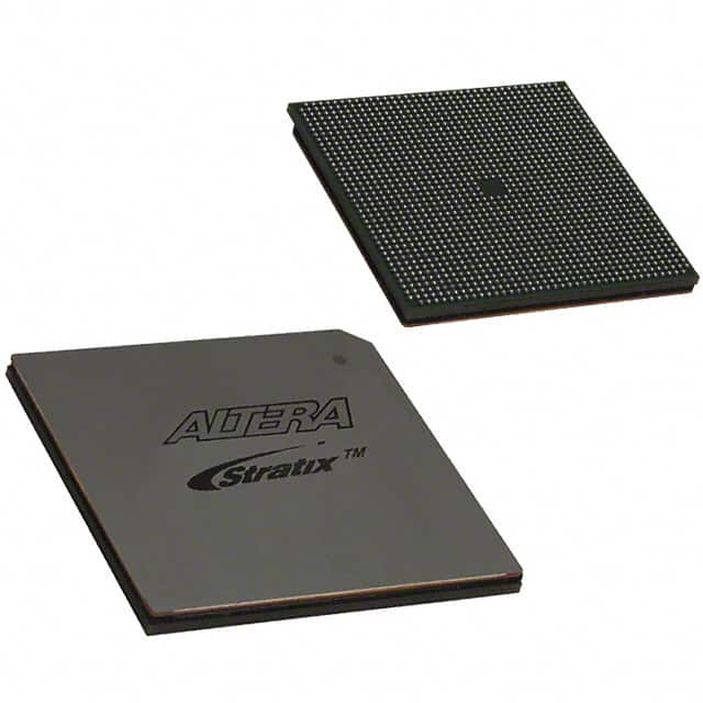
Lihat spesifikasi untuk detail produk.

EP1S40F1508C6
Basic Information Overview
- Category: Integrated Circuit (IC)
- Use: Programmable Logic Device (PLD)
- Characteristics: High-performance, low-power consumption, reprogrammable
- Package: 1508-ball FineLine BGA package
- Essence: A versatile PLD for various digital logic applications
- Packaging/Quantity: Typically sold in reels or trays containing multiple units
Specifications
- Technology: Field-Programmable Gate Array (FPGA)
- Logic Elements: 40,000
- Speed Grade: 6
- I/O Pins: 1508
- Operating Voltage: 1.2V
- Operating Temperature: -40°C to 100°C
- Package Dimensions: 35mm x 35mm
Detailed Pin Configuration
The EP1S40F1508C6 has a complex pin configuration with 1508 pins. For detailed pin assignments and functions, please refer to the manufacturer's datasheet.
Functional Features
- High-density integration of programmable logic elements
- Flexible and reprogrammable design allows for customization
- Low power consumption for energy-efficient operation
- Support for various communication protocols and interfaces
- On-chip memory blocks for efficient data storage
- Built-in clock management circuitry for precise timing control
Advantages
- Versatile and adaptable to different application requirements
- Reduced development time and cost compared to custom ASICs
- Easy prototyping and testing of digital logic designs
- Ability to make design changes even after deployment
- Availability of comprehensive development tools and support
Disadvantages
- Limited performance compared to dedicated ASICs
- Higher power consumption compared to specialized chips
- Relatively higher cost per unit compared to mass-produced ICs
- Complexity of programming and configuring the device
Working Principles
The EP1S40F1508C6 is based on FPGA technology, which utilizes a matrix of configurable logic blocks interconnected by programmable interconnects. These logic blocks can be programmed to implement various digital functions and perform complex computations. The device's configuration is stored in non-volatile memory cells, allowing it to retain the programmed design even after power-off.
Detailed Application Field Plans
The EP1S40F1508C6 finds applications in a wide range of fields, including: - Telecommunications: Signal processing, network routing, protocol conversion - Industrial Automation: Control systems, motor control, sensor interfacing - Consumer Electronics: High-definition video processing, audio codecs - Automotive: Engine control, driver assistance systems, infotainment - Aerospace: Avionics, satellite communication, radar systems
Detailed and Complete Alternative Models
- EP1S30F780C6: Smaller version with 30,000 logic elements and 780 I/O pins
- EP1S80F1020C6: Larger version with 80,000 logic elements and 1020 I/O pins
- EP2S180F1508C4: Higher-performance model with 180,000 logic elements and 1508 I/O pins
Please note that the above alternative models are just a few examples, and there are many more options available from the manufacturer.
This entry provides an overview of the EP1S40F1508C6, a versatile programmable logic device used in various digital logic applications. It includes information about its specifications, pin configuration, functional features, advantages, disadvantages, working principles, application field plans, and alternative models.
Sebutkan 10 pertanyaan dan jawaban umum terkait penerapan EP1S40F1508C6 dalam solusi teknis
Sure! Here are 10 common questions and answers related to the application of EP1S40F1508C6 in technical solutions:
Q1: What is EP1S40F1508C6? A1: EP1S40F1508C6 is a specific model of Field-Programmable Gate Array (FPGA) manufactured by Intel.
Q2: What are the key features of EP1S40F1508C6? A2: Some key features of EP1S40F1508C6 include 40,000 logic elements, 1.5V core voltage, and support for various I/O standards.
Q3: What are the typical applications of EP1S40F1508C6? A3: EP1S40F1508C6 is commonly used in applications such as digital signal processing, industrial automation, telecommunications, and high-performance computing.
Q4: How can EP1S40F1508C6 be programmed? A4: EP1S40F1508C6 can be programmed using hardware description languages (HDLs) like VHDL or Verilog, along with specialized software tools provided by Intel.
Q5: Can EP1S40F1508C6 be reprogrammed after initial programming? A5: Yes, EP1S40F1508C6 is a reprogrammable FPGA, allowing for multiple iterations of design implementation.
Q6: What are the power requirements for EP1S40F1508C6? A6: EP1S40F1508C6 requires a 1.5V core voltage and typically operates within a specified power supply range mentioned in the datasheet.
Q7: Does EP1S40F1508C6 support different I/O standards? A7: Yes, EP1S40F1508C6 supports various I/O standards such as LVCMOS, LVTTL, SSTL, and differential signaling standards like LVDS.
Q8: Can EP1S40F1508C6 interface with external memory devices? A8: Yes, EP1S40F1508C6 has dedicated pins and interfaces to connect with external memory devices like DDR SDRAM or SRAM.
Q9: What development tools are available for EP1S40F1508C6? A9: Intel provides Quartus Prime software suite, which includes design entry, synthesis, simulation, and programming tools specifically designed for programming EP1S40F1508C6.
Q10: Are there any reference designs or application notes available for EP1S40F1508C6? A10: Yes, Intel provides reference designs and application notes that can help users understand and implement EP1S40F1508C6 in various technical solutions. These resources can be found on the Intel website or through their support channels.
Please note that the answers provided here are general and may vary based on specific requirements and documentation provided by Intel for EP1S40F1508C6.

