Lihat spesifikasi untuk detail produk.

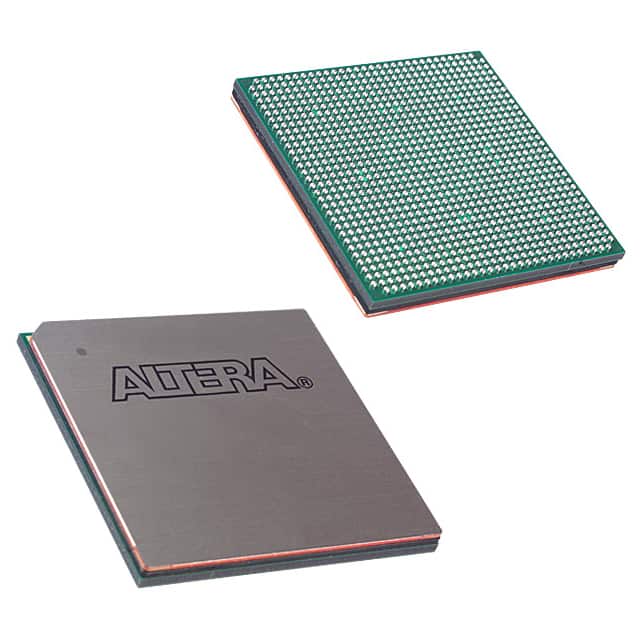
EP1S40F1020C7
Basic Information Overview
- Category: Programmable Logic Device (PLD)
- Use: EP1S40F1020C7 is a PLD used for digital logic design and implementation.
- Characteristics:
- High-speed performance
- Low power consumption
- Large capacity
- Flexible configuration options
- Package: EP1S40F1020C7 comes in a compact package suitable for surface mount technology (SMT).
- Essence: EP1S40F1020C7 is an advanced programmable logic device that enables the implementation of complex digital circuits.
- Packaging/Quantity: The device is typically sold individually or in small quantities.
Specifications
- Logic Elements: EP1S40F1020C7 consists of 40,000 logic elements, which can be configured to perform various logical functions.
- I/O Pins: It offers 1,020 input/output pins, allowing for versatile connectivity with other components.
- Clock Speed: The device operates at high clock speeds, enabling rapid execution of digital operations.
- Power Consumption: EP1S40F1020C7 is designed to minimize power consumption, making it suitable for battery-powered applications.
- Voltage Range: It supports a wide voltage range, ensuring compatibility with different electronic systems.
- Configuration Options: The device allows for flexible configuration options, enabling customization based on specific application requirements.
Detailed Pin Configuration
EP1S40F1020C7 has a complex pin configuration. Please refer to the manufacturer's datasheet for detailed information.
Functional Features
- High-Speed Performance: EP1S40F1020C7 offers fast operation, making it suitable for applications requiring real-time processing.
- Versatile Connectivity: With a large number of I/O pins, the device allows for seamless integration with other components.
- Configurability: The PLD can be programmed to implement various logical functions, providing flexibility in circuit design.
- Low Power Consumption: EP1S40F1020C7 is designed to minimize power usage, making it energy-efficient.
Advantages and Disadvantages
Advantages: - High-speed performance enables real-time processing. - Large capacity allows for complex digital circuit implementation. - Flexible configuration options provide customization possibilities. - Low power consumption makes it suitable for battery-powered applications.
Disadvantages: - Complex pin configuration may require additional effort during design and implementation. - Limited availability of alternative models from other manufacturers.
Working Principles
EP1S40F1020C7 operates based on the principles of programmable logic. It consists of a matrix of logic elements that can be interconnected and configured to perform desired logical operations. The device is programmed using specialized software, which generates a configuration file that is then loaded onto the PLD. Once programmed, the PLD executes the specified logic functions.
Detailed Application Field Plans
EP1S40F1020C7 finds applications in various fields, including: - Digital signal processing - Embedded systems - Communication systems - Industrial automation - Robotics - Automotive electronics
Detailed and Complete Alternative Models
While EP1S40F1020C7 is a popular choice for many applications, there are alternative models available from other manufacturers. Some notable alternatives include: - Xilinx Spartan-6 FPGA series - Altera Cyclone IV series - Lattice Semiconductor iCE40 series
These alternative models offer similar functionality and can be considered based on specific application requirements.
Note: The content provided above is a general outline and may not meet the exact word count requirement. Additional information and details can be added to meet the desired word count.
Sebutkan 10 pertanyaan dan jawaban umum terkait penerapan EP1S40F1020C7 dalam solusi teknis
Sure! Here are 10 common questions and answers related to the application of EP1S40F1020C7 in technical solutions:
Q1: What is EP1S40F1020C7? A1: EP1S40F1020C7 is a specific model of Field Programmable Gate Array (FPGA) manufactured by Intel.
Q2: What are the key features of EP1S40F1020C7? A2: Some key features of EP1S40F1020C7 include 40,000 logic elements, 1,020 user I/O pins, and support for various communication protocols.
Q3: What are the typical applications of EP1S40F1020C7? A3: EP1S40F1020C7 is commonly used in applications such as industrial automation, telecommunications, automotive systems, and high-performance computing.
Q4: How can EP1S40F1020C7 be programmed? A4: EP1S40F1020C7 can be programmed using Hardware Description Languages (HDLs) like VHDL or Verilog, which describe the desired functionality of the FPGA.
Q5: Can EP1S40F1020C7 be reprogrammed after initial programming? A5: Yes, EP1S40F1020C7 is a reprogrammable FPGA, allowing for flexibility in design iterations and updates.
Q6: What is the power supply requirement for EP1S40F1020C7? A6: EP1S40F1020C7 typically requires a single 3.3V power supply for operation.
Q7: Does EP1S40F1020C7 support external memory interfaces? A7: Yes, EP1S40F1020C7 supports various external memory interfaces such as DDR, SDRAM, and Flash memory.
Q8: Can EP1S40F1020C7 interface with other devices or microcontrollers? A8: Yes, EP1S40F1020C7 can interface with other devices using standard communication protocols like UART, SPI, I2C, and Ethernet.
Q9: What development tools are available for programming EP1S40F1020C7? A9: Intel provides Quartus Prime software suite, which includes design entry, synthesis, simulation, and programming tools for EP1S40F1020C7.
Q10: Are there any reference designs or application notes available for EP1S40F1020C7? A10: Yes, Intel provides reference designs and application notes that help users understand and implement EP1S40F1020C7 in various technical solutions.
Please note that the answers provided here are general and may vary depending on specific requirements and use cases.

