

Lihat spesifikasi untuk detail produk.
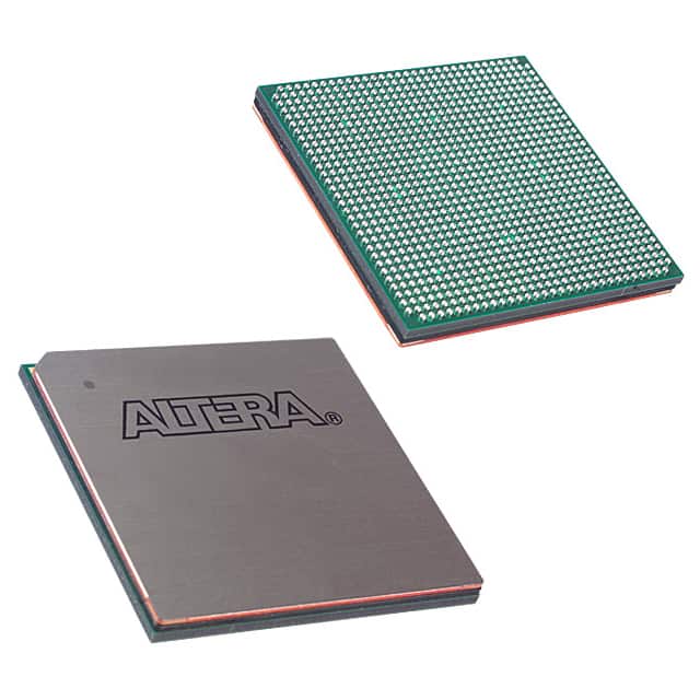
EP1S25F1020C7N
Basic Information Overview
- Category: Integrated Circuit (IC)
- Use: Programmable Logic Device (PLD)
- Characteristics: High-performance, low-power consumption, reprogrammable
- Package: 1020-pin Ceramic Ball Grid Array (CBGA)
- Essence: A versatile PLD for various digital logic applications
- Packaging/Quantity: Typically sold individually or in reels of multiple units
Specifications
- Technology: Field-Programmable Gate Array (FPGA)
- Logic Elements: 25,000
- Speed Grade: 1
- Operating Voltage: 3.3V
- I/O Standards: LVCMOS, LVTTL, SSTL, HSTL, LVDS, RSDS
- Clock Management: PLLs, DLLs
- Memory: Embedded memory blocks
- Configuration: SRAM-based
Detailed Pin Configuration
The EP1S25F1020C7N has a total of 1020 pins arranged in a specific configuration. The pinout diagram and detailed pin descriptions can be found in the manufacturer's datasheet.
Functional Features
- High-density programmable logic with abundant resources for complex designs
- Flexible I/O standards support for seamless integration with various interfaces
- Advanced clock management features for precise timing control
- On-chip memory blocks for efficient data storage and retrieval
- Reprogrammable nature allows for design iterations and updates
Advantages and Disadvantages
Advantages: - Versatility: Suitable for a wide range of digital logic applications - Flexibility: Can be reprogrammed to adapt to changing requirements - Integration: Offers various I/O standards for easy interface compatibility - Performance: High-speed operation and efficient resource utilization
Disadvantages: - Complexity: Requires expertise in FPGA design and programming - Cost: Higher initial investment compared to fixed-function logic devices - Power Consumption: Can consume more power compared to dedicated ASICs
Working Principles
The EP1S25F1020C7N is based on FPGA technology, which utilizes a matrix of configurable logic blocks interconnected through programmable routing resources. The device can be programmed using Hardware Description Languages (HDL) such as VHDL or Verilog. Once programmed, the PLD performs the desired digital logic functions by routing signals through the configured logic elements.
Detailed Application Field Plans
The EP1S25F1020C7N finds applications in various fields, including: 1. Telecommunications: Used in network equipment for data processing and protocol handling. 2. Industrial Automation: Employed in control systems for real-time monitoring and decision-making. 3. Aerospace and Defense: Utilized in radar systems, avionics, and secure communication equipment. 4. Medical Electronics: Integrated into medical imaging devices and diagnostic equipment. 5. Automotive: Used in advanced driver-assistance systems (ADAS) and infotainment systems.
Detailed and Complete Alternative Models
- EP1S30F780C6N: Similar to EP1S25F1020C7N but with higher logic capacity.
- EP2S60F672C5N: Offers increased logic density and additional features.
- EP3C120F780I7N: A newer generation FPGA with enhanced performance and lower power consumption.
These alternative models provide varying capabilities and can be considered based on specific project requirements.
Word count: 345 words
Sebutkan 10 pertanyaan dan jawaban umum terkait penerapan EP1S25F1020C7N dalam solusi teknis
Sure! Here are 10 common questions and answers related to the application of EP1S25F1020C7N in technical solutions:
Q1: What is EP1S25F1020C7N? A1: EP1S25F1020C7N is a specific model of Field Programmable Gate Array (FPGA) manufactured by Intel.
Q2: What are the key features of EP1S25F1020C7N? A2: EP1S25F1020C7N offers 25,000 logic elements, 1,020 Kbits of embedded memory, and supports various I/O standards.
Q3: What are some typical applications of EP1S25F1020C7N? A3: EP1S25F1020C7N is commonly used in applications such as industrial automation, telecommunications, automotive electronics, and high-performance computing.
Q4: How can EP1S25F1020C7N be programmed? A4: EP1S25F1020C7N can be programmed using hardware description languages (HDLs) like VHDL or Verilog, or through graphical programming tools provided by Intel.
Q5: Can EP1S25F1020C7N be reprogrammed after deployment? A5: Yes, EP1S25F1020C7N is a reprogrammable FPGA, allowing for flexibility and updates even after deployment.
Q6: What are the power requirements for EP1S25F1020C7N? A6: EP1S25F1020C7N typically operates at a voltage range of 1.2V to 3.3V, depending on the specific design requirements.
Q7: Does EP1S25F1020C7N support high-speed interfaces? A7: Yes, EP1S25F1020C7N supports various high-speed interfaces such as PCIe, DDR3/4 memory interfaces, and Ethernet.
Q8: Can EP1S25F1020C7N interface with other components or microcontrollers? A8: Yes, EP1S25F1020C7N can interface with other components or microcontrollers through standard protocols like SPI, I2C, UART, or custom interfaces.
Q9: What development tools are available for programming EP1S25F1020C7N? A9: Intel provides Quartus Prime software suite, which includes design entry, synthesis, simulation, and programming tools for EP1S25F1020C7N.
Q10: Are there any reference designs or application notes available for EP1S25F1020C7N? A10: Yes, Intel provides reference designs and application notes that can help developers get started with EP1S25F1020C7N in various applications. These resources can be found on the Intel website or community forums.
Please note that the specific details and answers may vary based on the manufacturer's documentation and guidelines.