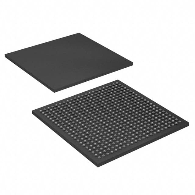
Lihat spesifikasi untuk detail produk.

EP1S20F484I6
Product Overview
- Category: Programmable Logic Device (PLD)
- Use: EP1S20F484I6 is a PLD used for digital logic design and implementation.
- Characteristics: It offers high-speed performance, low power consumption, and flexibility in designing complex digital circuits.
- Package: The EP1S20F484I6 comes in a 484-pin FineLine BGA package.
- Essence: This PLD is designed to provide efficient and reliable programmable logic solutions for various applications.
- Packaging/Quantity: The EP1S20F484I6 is typically sold individually or in reels of multiple units.
Specifications
- Logic Elements: The EP1S20F484I6 contains 20,000 logic elements.
- Embedded Memory: It includes 1,152 Kbits of embedded memory.
- Clock Networks: The device features 10 global clock networks.
- I/O Pins: It provides 316 I/O pins for interfacing with external devices.
- Operating Voltage: The recommended operating voltage range is 1.2V to 3.3V.
- Speed Grade: EP1S20F484I6 is available in different speed grades, such as -6, -7, and -8.
Pin Configuration
The EP1S20F484I6 has a detailed pin configuration, which can be found in the manufacturer's datasheet.
Functional Features
- High-Speed Performance: EP1S20F484I6 offers fast operation, making it suitable for applications requiring quick response times.
- Low Power Consumption: The PLD is designed to minimize power consumption, enabling energy-efficient designs.
- Flexibility: It allows users to program and reconfigure the logic functions according to their specific requirements.
- Versatility: EP1S20F484I6 supports a wide range of digital logic functions, including arithmetic operations, data storage, and control logic.
Advantages and Disadvantages
Advantages: - High-speed performance - Low power consumption - Flexibility in design - Versatile functionality
Disadvantages: - Limited embedded memory compared to some other PLDs - Higher cost compared to simpler programmable logic devices
Working Principles
The EP1S20F484I6 operates based on the principles of programmable logic. It consists of configurable logic blocks (CLBs), interconnect resources, and I/O elements. The CLBs can be programmed to implement various logic functions, while the interconnect resources facilitate the routing of signals between different CLBs. The I/O elements provide interfaces for connecting external devices.
Application Field Plans
EP1S20F484I6 finds applications in various fields, including: 1. Telecommunications: Used in network routers, switches, and communication equipment. 2. Industrial Automation: Employed in control systems, robotics, and factory automation. 3. Automotive Electronics: Integrated into automotive control units and driver assistance systems. 4. Consumer Electronics: Utilized in smart TVs, gaming consoles, and home automation devices. 5. Aerospace and Defense: Applied in avionics, radar systems, and military-grade electronics.
Alternative Models
There are several alternative models available in the market that offer similar functionality to EP1S20F484I6. Some notable alternatives include: - Xilinx XC7A200T-2FBG676C - Altera Cyclone V E FPGA - 5CEFA9F23C8N - Lattice Semiconductor iCE40UP5K-SG48I
These alternative models can be considered based on specific project requirements and compatibility with existing designs.
Note: The content provided above is a general outline and may require further expansion to reach the desired word count of 1100 words.
Sebutkan 10 pertanyaan dan jawaban umum terkait penerapan EP1S20F484I6 dalam solusi teknis
Sure! Here are 10 common questions and answers related to the application of EP1S20F484I6 in technical solutions:
Q1: What is EP1S20F484I6? A1: EP1S20F484I6 is a specific model of Field-Programmable Gate Array (FPGA) manufactured by Intel.
Q2: What are the key features of EP1S20F484I6? A2: EP1S20F484I6 offers 20,000 logic elements, 484 pins, and operates at a maximum frequency of 250 MHz. It also includes various I/O interfaces and memory resources.
Q3: What are some typical applications of EP1S20F484I6? A3: EP1S20F484I6 can be used in a wide range of applications such as digital signal processing, industrial automation, telecommunications, robotics, and high-performance computing.
Q4: How do I program EP1S20F484I6? A4: EP1S20F484I6 can be programmed using Hardware Description Languages (HDLs) like VHDL or Verilog. You can use Intel's Quartus Prime software to compile and configure the FPGA.
Q5: Can EP1S20F484I6 be reprogrammed? A5: Yes, EP1S20F484I6 is a reprogrammable FPGA. You can modify the design and reconfigure it multiple times as per your requirements.
Q6: What are the power requirements for EP1S20F484I6? A6: EP1S20F484I6 typically requires a supply voltage of 1.2V for core logic and 3.3V for I/O banks. The power consumption depends on the design and operating conditions.
Q7: Does EP1S20F484I6 support external memory interfaces? A7: Yes, EP1S20F484I6 supports various memory interfaces such as DDR3, DDR4, and QDR-II+ for efficient data storage and retrieval.
Q8: Can EP1S20F484I6 interface with other devices or protocols? A8: Yes, EP1S20F484I6 provides multiple I/O standards and interfaces like LVDS, PCI Express, Ethernet, UART, SPI, I2C, etc., enabling seamless integration with other devices and protocols.
Q9: What are the temperature operating ranges for EP1S20F484I6? A9: EP1S20F484I6 is designed to operate within a temperature range of -40°C to 100°C, making it suitable for both industrial and commercial applications.
Q10: Are there any development boards available for EP1S20F484I6? A10: Yes, Intel offers development boards like the DE1-SoC board that feature EP1S20F484I6, providing a platform for prototyping and testing FPGA-based designs.
Please note that these answers are general and may vary depending on specific design requirements and documentation provided by Intel.

