Lihat spesifikasi untuk detail produk.

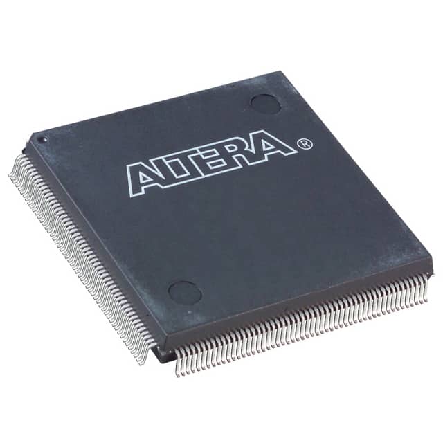
EP1K10QC208-2
Product Overview
Category: Integrated Circuit (IC)
Use: The EP1K10QC208-2 is a programmable logic device (PLD) that belongs to the EP1K family of devices manufactured by Altera Corporation. It is designed for use in various digital applications, including telecommunications, industrial automation, consumer electronics, and more.
Characteristics: - High-performance PLD with advanced features - Low power consumption - Compact size - Flexible and versatile design
Package: The EP1K10QC208-2 is available in a Quad Flat Package (QFP), which provides ease of installation and compatibility with standard PCB designs.
Essence: This PLD is built using advanced semiconductor technology, allowing for efficient and reliable digital circuit implementation.
Packaging/Quantity: The EP1K10QC208-2 is typically packaged in reels or trays, containing a specific quantity of devices per package. The exact packaging and quantity may vary depending on the supplier.
Specifications
The EP1K10QC208-2 offers the following specifications:
- Logic Elements: 10,000
- Maximum User I/Os: 173
- Embedded Multiplier Blocks: 20
- Maximum Operating Frequency: 200 MHz
- On-Chip Memory: 288 Kbits
- Supply Voltage: 3.3V
- Operating Temperature Range: -40°C to +85°C
Pin Configuration
The EP1K10QC208-2 has a total of 208 pins, each serving a specific function within the device. The detailed pin configuration can be found in the manufacturer's datasheet.
Functional Features
The EP1K10QC208-2 offers several functional features that enhance its usability and performance:
- Programmability: The device can be programmed to implement various digital logic functions, allowing for customization and adaptability.
- High-Speed Operation: With a maximum operating frequency of 200 MHz, the EP1K10QC208-2 can handle demanding applications that require fast data processing.
- Embedded Multiplier Blocks: The presence of 20 embedded multiplier blocks enables efficient multiplication operations within the device, reducing the need for external components.
- On-Chip Memory: The built-in 288 Kbits of memory provide storage capacity for data and configuration information, eliminating the need for external memory devices.
Advantages and Disadvantages
Advantages: - Versatile and flexible design allows for a wide range of applications - Low power consumption contributes to energy efficiency - Compact size saves valuable PCB space - High-performance capabilities enable complex digital circuit implementation
Disadvantages: - Limited logic elements compared to higher-end PLDs - Higher cost compared to simpler programmable logic devices
Working Principles
The EP1K10QC208-2 operates based on the principles of programmable logic. It consists of configurable logic blocks (CLBs), interconnect resources, I/O elements, and other supporting components. The device is programmed using hardware description languages (HDLs) or graphical design tools, which define the desired digital logic functionality. Once programmed, the EP1K10QC208-2 executes the specified logic operations, enabling the desired behavior in the target application.
Application Field Plans
The EP1K10QC208-2 finds applications in various fields, including:
- Telecommunications: Used in network routers, switches, and communication equipment for high-speed data processing and protocol handling.
- Industrial Automation: Employed in control systems, PLCs, and robotics for implementing complex logic functions and interfacing with sensors and actuators.
- Consumer Electronics: Integrated into smart home devices, gaming consoles, and multimedia systems for efficient data processing and control.
- Automotive: Utilized in automotive electronics for functions such as engine management, driver assistance systems, and infotainment.
Alternative Models
For those seeking alternative options, the following models can be considered:
- EP1K30QC208-2: Offers higher logic capacity (30,000 logic elements) for more complex applications.
- EP1K10TC144-3: Provides a different package option (TQFP) with 144 pins, suitable for space-constrained designs.
- EP1K50QC208-2: Offers increased I/O count (up to 346) for applications requiring extensive interfacing capabilities.
These alternative models provide varying features and specifications to cater to specific application requirements.
In conclusion, the EP1K10QC208-2 is a versatile and high-performance programmable logic device that finds applications in diverse fields. Its compact size, low power consumption, and advanced features make it an attractive choice for digital circuit implementation.
Sebutkan 10 pertanyaan dan jawaban umum terkait penerapan EP1K10QC208-2 dalam solusi teknis
Sure! Here are 10 common questions and answers related to the application of EP1K10QC208-2 in technical solutions:
Q1: What is EP1K10QC208-2? A1: EP1K10QC208-2 is a specific model of field-programmable gate array (FPGA) manufactured by Altera.
Q2: What are the key features of EP1K10QC208-2? A2: EP1K10QC208-2 has 10,000 logic elements, 208 pins, and operates at a maximum frequency of 200 MHz. It also includes built-in memory blocks and digital signal processing (DSP) capabilities.
Q3: What are some typical applications of EP1K10QC208-2? A3: EP1K10QC208-2 can be used in various technical solutions such as industrial automation, telecommunications, image and video processing, robotics, and embedded systems.
Q4: How can EP1K10QC208-2 be programmed? A4: EP1K10QC208-2 can be programmed using hardware description languages (HDLs) like VHDL or Verilog, or through graphical programming tools provided by Altera.
Q5: Can EP1K10QC208-2 be reprogrammed after deployment? A5: Yes, EP1K10QC208-2 is a field-programmable device, which means it can be reprogrammed even after it has been deployed in a system.
Q6: What are the power requirements for EP1K10QC208-2? A6: EP1K10QC208-2 typically requires a supply voltage of 3.3V and consumes power based on the complexity of the design implemented on the FPGA.
Q7: Does EP1K10QC208-2 support external memory interfaces? A7: Yes, EP1K10QC208-2 supports various external memory interfaces such as SDRAM, DDR, and flash memory.
Q8: Can EP1K10QC208-2 communicate with other devices or microcontrollers? A8: Yes, EP1K10QC208-2 can communicate with other devices or microcontrollers through various communication protocols like UART, SPI, I2C, or Ethernet.
Q9: Are there any development boards available for EP1K10QC208-2? A9: Yes, Altera provides development boards specifically designed for EP1K10QC208-2, which include necessary connectors, peripherals, and programming interfaces.
Q10: Where can I find technical documentation and support for EP1K10QC208-2? A10: You can find technical documentation, datasheets, application notes, and support resources for EP1K10QC208-2 on the official website of Altera (now Intel FPGA) or by contacting their customer support.

