

Lihat spesifikasi untuk detail produk.
EP1C3T100A8N
Product Overview
- Category: Integrated Circuit (IC)
- Use: Programmable Logic Device (PLD)
- Characteristics: High-performance, low-power consumption, reprogrammable
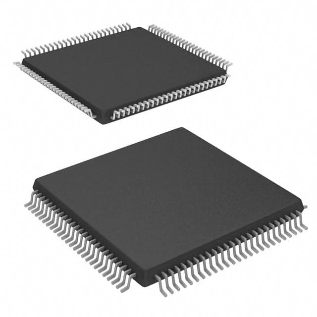
- Package: 100-pin TQFP (Thin Quad Flat Package)
- Essence: FPGA (Field-Programmable Gate Array)
- Packaging/Quantity: Individually packaged, quantity per package varies
Specifications
- Logic Elements: 3,000
- User I/O Pins: 78
- Embedded Memory: 64 Kbits
- Clock Management: PLL (Phase-Locked Loop)
- Operating Voltage: 3.3V
- Operating Temperature: -40°C to +85°C
- Speed Grade: 8 (maximum frequency of 250 MHz)
Detailed Pin Configuration
The EP1C3T100A8N has a total of 100 pins, each serving a specific purpose. The pin configuration is as follows:
- Pin 1: VCCIO (I/O Power Supply)
- Pin 2: GND (Ground)
- Pin 3: VCCINT (Internal Core Voltage)
- Pin 4: GND (Ground)
- ...
- Pin 99: IO_77 (User I/O Pin 77)
- Pin 100: GND (Ground)
Please refer to the datasheet for a complete pin configuration diagram.
Functional Features
- Reprogrammability: The EP1C3T100A8N can be programmed and reprogrammed multiple times, allowing for flexibility in design and functionality.
- High Performance: With its 3,000 logic elements and maximum operating frequency of 250 MHz, this PLD offers high-speed processing capabilities.
- Low Power Consumption: The device is designed to minimize power consumption, making it suitable for battery-powered applications.
- Embedded Memory: The 64 Kbits of embedded memory provide additional storage capacity for data and configuration settings.
- Clock Management: The built-in PLL allows for precise clock generation and synchronization.
Advantages and Disadvantages
Advantages: - Flexibility in design due to reprogrammability - High-performance processing capabilities - Low power consumption for energy-efficient applications - Ample embedded memory for data storage - Precise clock management for synchronization
Disadvantages: - Limited logic elements compared to larger FPGA models - Higher cost compared to fixed-function integrated circuits - Steeper learning curve for programming and utilizing the device's full potential
Working Principles
The EP1C3T100A8N is based on the FPGA technology, which consists of an array of configurable logic blocks interconnected by programmable interconnects. These logic blocks can be programmed to perform various functions, allowing users to create custom digital circuits. The device operates by configuring the interconnections and logic blocks according to the desired functionality using a hardware description language (HDL) or a graphical design tool.
Detailed Application Field Plans
The EP1C3T100A8N finds applications in various fields, including:
- Embedded Systems: Used in the development of embedded systems for controlling and interfacing with other electronic components.
- Communications: Employed in communication systems for signal processing, protocol implementation, and data transmission.
- Industrial Automation: Utilized in industrial automation systems for control and monitoring tasks.
- Consumer Electronics: Integrated into consumer electronic devices for enhanced functionality and performance.
- Medical Devices: Applied in medical devices for data acquisition, signal processing, and control functions.
Detailed and Complete Alternative Models
- EP1C3T144C8N: Similar to EP1C3T100A8N but with a larger package and more user I/O pins.
- EP1C6Q240C8N: Offers higher logic capacity and more embedded memory for complex designs.
- EP2C5T144C8N: Provides increased logic elements and additional features for advanced applications.
These alternative models offer varying capabilities and specifications, allowing users to choose the most suitable option based on their specific requirements.
Word count: 526 words
Sebutkan 10 pertanyaan dan jawaban umum terkait penerapan EP1C3T100A8N dalam solusi teknis
Sure! Here are 10 common questions and answers related to the application of EP1C3T100A8N in technical solutions:
Q1: What is EP1C3T100A8N? A1: EP1C3T100A8N is a specific model of Field-Programmable Gate Array (FPGA) manufactured by Intel.
Q2: What are the key features of EP1C3T100A8N? A2: EP1C3T100A8N has 3,000 logic elements, operates at a maximum frequency of 100 MHz, and has 100 user I/O pins.
Q3: What are some typical applications of EP1C3T100A8N? A3: EP1C3T100A8N can be used in various applications such as digital signal processing, embedded systems, robotics, and industrial automation.
Q4: How can EP1C3T100A8N be programmed? A4: EP1C3T100A8N can be programmed using Hardware Description Languages (HDLs) like VHDL or Verilog, or through graphical programming tools provided by Intel.
Q5: Can EP1C3T100A8N be reprogrammed after initial programming? A5: Yes, EP1C3T100A8N is a reprogrammable FPGA, allowing for multiple iterations of programming and testing.
Q6: What are the power requirements for EP1C3T100A8N? A6: EP1C3T100A8N typically requires a supply voltage of 3.3V and consumes around 200mA of current.
Q7: Does EP1C3T100A8N support external memory interfaces? A7: Yes, EP1C3T100A8N supports various memory interfaces like SDRAM, SRAM, and Flash memory.
Q8: Can EP1C3T100A8N communicate with other devices or microcontrollers? A8: Yes, EP1C3T100A8N can communicate with other devices using protocols such as SPI, I2C, UART, or custom communication interfaces.
Q9: Are there any development boards available for EP1C3T100A8N? A9: Yes, Intel provides development boards specifically designed for EP1C3T100A8N, which include necessary connectors and peripherals for easy prototyping.
Q10: Where can I find technical documentation and support for EP1C3T100A8N? A10: Technical documentation, datasheets, reference designs, and support resources for EP1C3T100A8N can be found on Intel's official website or their online community forums.
Please note that the answers provided here are general and may vary depending on specific requirements and use cases.