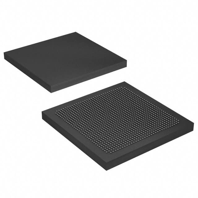
Lihat spesifikasi untuk detail produk.

5SGXMA5H2F35I3LN
Product Overview
- Category: Integrated Circuit (IC)
- Use: Programmable Logic Device (PLD)
- Characteristics: High-performance, low-power consumption
- Package: BGA (Ball Grid Array)
- Essence: FPGA (Field-Programmable Gate Array)
- Packaging/Quantity: Single unit
Specifications
- Manufacturer: Intel Corporation
- Family: Stratix V
- Device Name: 5SGXMA5H2F35I3LN
- Logic Elements: 220,000
- Embedded Memory: 8,100 Kbits
- Maximum User I/O Pins: 1,280
- Operating Voltage: 1.0V
- Operating Temperature: -40°C to +100°C
- Package Size: 35mm x 35mm
- Package Type: F35 (1152-pin BGA)
Detailed Pin Configuration
The 5SGXMA5H2F35I3LN has a total of 1,152 pins arranged in a Ball Grid Array (BGA) package. The pin configuration includes various types of pins such as power supply pins, ground pins, input/output pins, clock pins, and configuration pins. Each pin serves a specific purpose and is labeled accordingly.
For the detailed pin configuration diagram, please refer to the manufacturer's datasheet.
Functional Features
- High-performance FPGA with advanced architecture
- Low-power consumption for energy-efficient applications
- Large number of logic elements for complex designs
- Embedded memory blocks for data storage
- High-speed transceivers for high-bandwidth communication
- Flexible I/O options for versatile connectivity
- Support for various industry-standard interfaces
- Configurable through programming for custom functionality
Advantages and Disadvantages
Advantages: - High-performance capabilities for demanding applications - Flexibility to adapt to changing design requirements - Low-power consumption for energy-efficient operation - Large number of logic elements for complex designs - Support for various industry-standard interfaces
Disadvantages: - Relatively high cost compared to other programmable logic devices - Steeper learning curve for beginners due to complexity - Limited availability of alternative models with similar specifications
Working Principles
The 5SGXMA5H2F35I3LN is a Field-Programmable Gate Array (FPGA) that operates based on the principles of digital logic. It consists of an array of configurable logic blocks interconnected through programmable routing resources. The device can be programmed to implement custom digital circuits by configuring the interconnections and functionality of its logic elements.
The FPGA's configuration is stored in non-volatile memory, allowing it to retain the programmed design even after power is removed. During operation, the FPGA executes the configured logic, performing tasks such as data processing, signal generation, and control functions.
Detailed Application Field Plans
The 5SGXMA5H2F35I3LN FPGA is widely used in various application fields, including:
- Communications: Used in networking equipment, routers, and switches for high-speed data processing and packet forwarding.
- Industrial Automation: Employed in industrial control systems, robotics, and factory automation for real-time control and monitoring.
- Medical Devices: Utilized in medical imaging systems, patient monitoring devices, and diagnostic equipment for data processing and analysis.
- Aerospace and Defense: Integrated into avionics systems, radar systems, and military communication equipment for high-performance computing and signal processing.
- Automotive: Applied in advanced driver-assistance systems (ADAS), infotainment systems, and engine control units (ECUs) for enhanced functionality and performance.
Detailed and Complete Alternative Models
While the 5SGXMA5H2F35I3LN offers a unique combination of specifications, there are alternative models available from other manufacturers that offer similar capabilities. Some notable alternatives include:
- Xilinx Virtex-7 XC7VX690T: Offers comparable logic capacity and I/O capabilities.
- LatticeECP5 LFE5UM-85F: Provides similar power efficiency and embedded memory capacity.
- Microsemi SmartFusion2 M2S150: Combines FPGA fabric with integrated ARM Cortex-M3 processor for added flexibility.
These alternative models can be considered based on specific project requirements and cost considerations.
Word count: 518 words
Sebutkan 10 pertanyaan dan jawaban umum terkait penerapan 5SGXMA5H2F35I3LN dalam solusi teknis
Sure! Here are 10 common questions and answers related to the application of 5SGXMA5H2F35I3LN in technical solutions:
Question: What is the maximum number of logic elements available in the 5SGXMA5H2F35I3LN FPGA?
- Answer: The 5SGXMA5H2F35I3LN FPGA has a maximum of 462,000 logic elements.Question: Can I use this FPGA for high-speed data processing applications?
- Answer: Yes, the 5SGXMA5H2F35I3LN FPGA is suitable for high-speed data processing due to its advanced architecture and high-performance features.Question: Does this FPGA support PCIe connectivity?
- Answer: Yes, the 5SGXMA5H2F35I3LN FPGA supports PCIe Gen1, Gen2, and Gen3 interfaces, making it compatible with various systems.Question: What is the maximum number of transceivers available in this FPGA?
- Answer: The 5SGXMA5H2F35I3LN FPGA has a total of 96 transceivers, which can be used for high-speed serial communication.Question: Can I implement DSP algorithms using this FPGA?
- Answer: Absolutely! The 5SGXMA5H2F35I3LN FPGA provides dedicated DSP blocks that enable efficient implementation of digital signal processing algorithms.Question: Is there any built-in memory available in this FPGA?
- Answer: Yes, the 5SGXMA5H2F35I3LN FPGA includes embedded memory blocks (RAM) that can be used for storing data within the device.Question: Can I interface this FPGA with external memory devices?
- Answer: Yes, the 5SGXMA5H2F35I3LN FPGA supports various memory interfaces such as DDR3, DDR4, QDR II+, and RLDRAM III, allowing you to connect external memory devices.Question: What is the maximum number of I/O pins available in this FPGA?
- Answer: The 5SGXMA5H2F35I3LN FPGA provides a total of 1,080 I/O pins, which can be used for interfacing with external components.Question: Can I use this FPGA for video processing applications?
- Answer: Yes, the 5SGXMA5H2F35I3LN FPGA offers dedicated video processing capabilities, including video input/output interfaces and hardware accelerators.Question: Is there any development kit available for this FPGA?
- Answer: Yes, Intel (formerly Altera) provides development kits specifically designed for the 5SGXMA5H2F35I3LN FPGA, which include necessary tools, documentation, and example designs to facilitate development.

