

Lihat spesifikasi untuk detail produk.
5SGXMA3H2F35I3LN
Product Overview
Category
The 5SGXMA3H2F35I3LN belongs to the category of Field Programmable Gate Arrays (FPGAs).
Use
This FPGA is designed for high-performance applications that require complex digital logic circuits. It provides a flexible and reconfigurable hardware platform for various electronic systems.
Characteristics
- High-speed processing capabilities
- Large number of programmable logic elements
- On-chip memory resources
- Flexible I/O interfaces
- Low power consumption
- High reliability
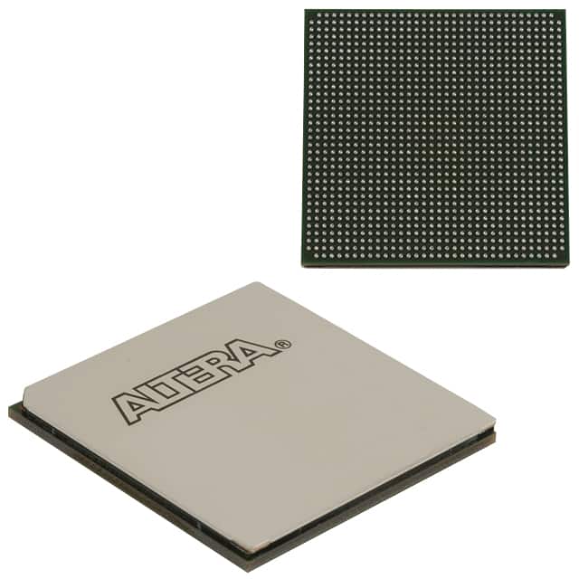
Package
The 5SGXMA3H2F35I3LN comes in a compact package suitable for surface mount technology (SMT) assembly. The package ensures easy integration into electronic systems.
Essence
The essence of this FPGA lies in its ability to implement complex digital logic functions using programmable interconnects and configurable logic blocks. It enables designers to create custom hardware solutions without the need for dedicated application-specific integrated circuits (ASICs).
Packaging/Quantity
The 5SGXMA3H2F35I3LN is typically packaged in trays or reels, depending on the manufacturer's specifications. The quantity per package may vary, but it is commonly available in quantities suitable for both prototyping and production purposes.
Specifications
- Logic Elements: 220,000
- Embedded Memory: 8,000 Kbits
- DSP Blocks: 1,526
- Maximum User I/O Pins: 622
- Operating Voltage: 1.2V
- Operating Temperature Range: -40°C to 100°C
- Package Type: F35 (1152-pin FineLine BGA)
Detailed Pin Configuration
The detailed pin configuration of the 5SGXMA3H2F35I3LN can be found in the product datasheet provided by the manufacturer. It includes information on power supply pins, I/O pins, configuration pins, and other specialized pins.
Functional Features
- High-speed data processing
- Configurable logic blocks for implementing custom digital circuits
- On-chip memory resources for efficient data storage
- Flexible I/O interfaces for seamless integration with external devices
- Built-in DSP blocks for signal processing applications
- Support for various communication protocols
- Advanced clock management features for precise timing control
Advantages and Disadvantages
Advantages
- Flexibility: The FPGA can be reprogrammed to adapt to changing requirements.
- Cost-effectiveness: Eliminates the need for dedicated ASICs, reducing development costs.
- Time-to-market: Allows rapid prototyping and faster product development cycles.
- High-performance: Capable of handling complex computations and real-time processing.
- Power efficiency: Optimized power consumption compared to traditional hardware solutions.
Disadvantages
- Complexity: Designing and programming FPGAs requires specialized knowledge and skills.
- Limited resources: The available logic elements and memory may impose constraints on certain applications.
- Higher cost per unit compared to mass-produced ASICs for large-scale production.
Working Principles
The 5SGXMA3H2F35I3LN operates based on the principles of configurable logic and programmable interconnects. The logic elements can be programmed to implement desired digital functions, while the interconnects allow for flexible routing of signals between these elements. The FPGA's configuration is stored in non-volatile memory and can be modified as needed.
Detailed Application Field Plans
The 5SGXMA3H2F35I3LN finds applications in various fields, including:
- Telecommunications: Used in base stations, network routers, and switches for high-speed data processing and protocol handling.
- Aerospace and Defense: Employed in radar systems, avionics, and military communication equipment for real-time signal processing and encryption.
- Industrial Automation: Utilized in control systems, robotics, and machine vision applications for high-performance data processing and sensor interfacing.
- Medical Devices: Integrated into medical imaging systems, patient monitoring devices, and diagnostic equipment for efficient data processing and analysis.
- Automotive: Used in advanced driver-assistance systems (ADAS), infotainment systems, and engine control units (ECUs) for real-time processing and connectivity.
Detailed and Complete Alternative Models
- 5SGXEA7K2F40C2N: Similar FPGA with higher logic capacity and additional features.
- 5SGXEB6R2F40I3N: FPGA with lower logic capacity but optimized for power efficiency.
- 5SGXMA5H2F35C2LN: FPGA with similar logic capacity but enhanced memory resources.
- 5SGXBA9H2F35I3LN: FPGA with higher I/O pin count and specialized interfaces for specific applications.
These alternative models offer different trade-offs in terms of logic capacity
Sebutkan 10 pertanyaan dan jawaban umum terkait penerapan 5SGXMA3H2F35I3LN dalam solusi teknis
Sure! Here are 10 common questions and answers related to the application of 5SGXMA3H2F35I3LN in technical solutions:
Question: What is the 5SGXMA3H2F35I3LN FPGA used for?
- Answer: The 5SGXMA3H2F35I3LN FPGA is commonly used for high-performance applications that require advanced processing capabilities.Question: What are some typical applications for this FPGA?
- Answer: Some typical applications include telecommunications, networking, industrial automation, video processing, and high-performance computing.Question: What are the key features of the 5SGXMA3H2F35I3LN FPGA?
- Answer: Key features include a large number of logic elements, high-speed transceivers, embedded memory blocks, and support for various communication protocols.Question: Can this FPGA handle high-speed data transfer?
- Answer: Yes, the 5SGXMA3H2F35I3LN FPGA has high-speed transceivers that can handle data rates up to several gigabits per second.Question: Does this FPGA support multiple communication protocols?
- Answer: Yes, it supports various communication protocols such as PCIe, Ethernet, USB, and DDR3/DDR4 memory interfaces.Question: How much logic capacity does this FPGA have?
- Answer: The 5SGXMA3H2F35I3LN FPGA has a logic capacity of approximately 3 million equivalent LEs (Logic Elements).Question: Can I program this FPGA using popular design tools?
- Answer: Yes, this FPGA is compatible with popular design tools like Quartus Prime from Intel.Question: Is there any built-in memory available in this FPGA?
- Answer: Yes, the 5SGXMA3H2F35I3LN FPGA has embedded memory blocks that can be used for storing data or implementing complex algorithms.Question: Can I interface this FPGA with external devices?
- Answer: Absolutely! This FPGA provides various I/O options, including LVDS, GPIOs, and high-speed transceivers, allowing easy interfacing with external devices.Question: What is the power consumption of this FPGA?
- Answer: The power consumption of the 5SGXMA3H2F35I3LN FPGA depends on the specific design and usage scenario, but it is generally designed to be power-efficient.
Please note that the specific details and answers may vary depending on the context and application requirements.