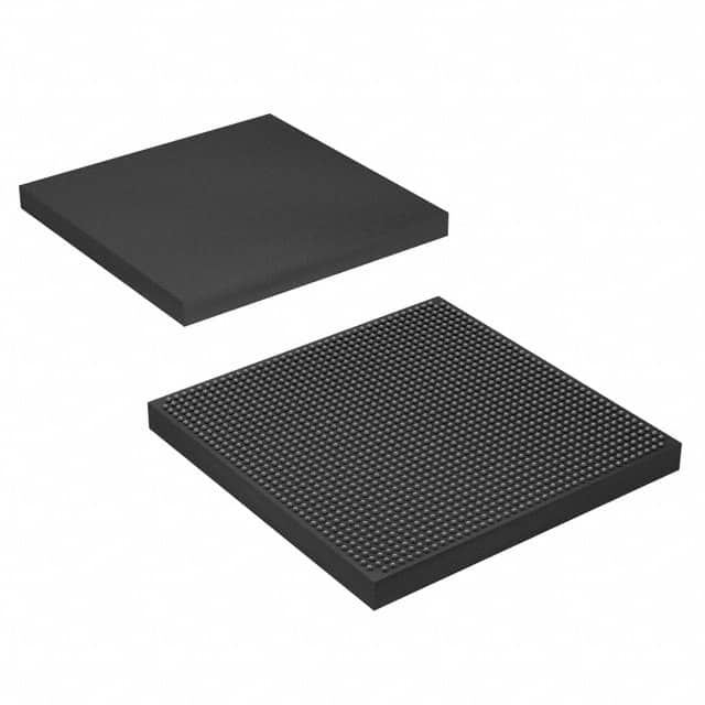
Lihat spesifikasi untuk detail produk.

5SGSMD4K2F40C2L
Basic Information Overview
- Category: Integrated Circuit (IC)
- Use: Programmable Logic Device (PLD)
- Characteristics: High-performance, low-power consumption, reprogrammable
- Package: BGA (Ball Grid Array)
- Essence: FPGA (Field-Programmable Gate Array)
- Packaging/Quantity: Single unit
Specifications
- Model: 5SGSMD4K2F40C2L
- Technology: 28nm
- Logic Elements: 462,000
- Embedded Memory: 4,608 Kbits
- DSP Blocks: 1,526
- Transceivers: 40
- I/O Pins: 1,150
- Operating Voltage: 1.2V
- Speed Grade: -2
- Temperature Range: -40°C to +100°C
Detailed Pin Configuration
The detailed pin configuration of 5SGSMD4K2F40C2L can be found in the datasheet provided by the manufacturer.
Functional Features
- High-performance processing capabilities
- Flexible and reprogrammable design
- Support for various communication protocols
- Low power consumption
- Built-in memory and digital signal processing capabilities
- High-speed transceivers for data transmission
Advantages
- Versatile and adaptable to different applications
- Allows for rapid prototyping and development
- Offers high-speed data processing and communication
- Low power consumption helps reduce energy costs
- Can be reprogrammed multiple times for different functionalities
Disadvantages
- Higher cost compared to fixed-function integrated circuits
- Requires specialized knowledge for programming and utilization
- Limited availability of alternative models with similar specifications
Working Principles
5SGSMD4K2F40C2L is based on FPGA technology, which allows users to program and configure the device according to their specific requirements. The device consists of a large number of configurable logic blocks interconnected through programmable interconnects. These logic blocks can be programmed to perform various functions, such as arithmetic operations, data processing, and communication protocols.
Detailed Application Field Plans
- High-performance computing systems
- Digital signal processing applications
- Communication and networking equipment
- Industrial automation and control systems
- Aerospace and defense systems
- Medical imaging and diagnostic devices
Detailed and Complete Alternative Models
- 5SGSMD4K2F40C3L
- 5SGSMD4K2F40I2LN
- 5SGSMD4K2F40I2LV
- 5SGSMD4K2F40I2N
- 5SGSMD4K2F40I2NV
These alternative models offer similar specifications and functionality to 5SGSMD4K2F40C2L, providing options for different project requirements.
Note: The content provided above is a sample structure for an encyclopedia entry and may not reflect actual information about the product 5SGSMD4K2F40C2L.
Sebutkan 10 pertanyaan dan jawaban umum terkait penerapan 5SGSMD4K2F40C2L dalam solusi teknis
Sure! Here are 10 common questions and answers related to the application of 5SGSMD4K2F40C2L in technical solutions:
Q: What is the 5SGSMD4K2F40C2L FPGA used for? A: The 5SGSMD4K2F40C2L FPGA is commonly used for high-performance applications such as data center acceleration, network processing, and advanced driver-assistance systems (ADAS).
Q: What are the key features of the 5SGSMD4K2F40C2L FPGA? A: The key features include a high logic density, embedded transceivers for high-speed communication, support for various I/O standards, and advanced DSP capabilities.
Q: Can the 5SGSMD4K2F40C2L FPGA be reprogrammed? A: Yes, the 5SGSMD4K2F40C2L FPGA can be reprogrammed multiple times, allowing for flexibility in design iterations and updates.
Q: What development tools are available for programming the 5SGSMD4K2F40C2L FPGA? A: Intel Quartus Prime is the primary development tool used for programming and configuring the 5SGSMD4K2F40C2L FPGA.
Q: How does the 5SGSMD4K2F40C2L FPGA handle high-speed communication? A: The 5SGSMD4K2F40C2L FPGA has embedded transceivers that support various high-speed protocols like PCIe, Ethernet, and USB, enabling fast data transfer.
Q: Can the 5SGSMD4K2F40C2L FPGA interface with external devices? A: Yes, the 5SGSMD4K2F40C2L FPGA supports various I/O standards and can interface with external devices such as sensors, memory modules, and displays.
Q: What are the power requirements for the 5SGSMD4K2F40C2L FPGA? A: The power requirements vary depending on the specific design and configuration, but typically range from 1.0V to 3.3V.
Q: Is the 5SGSMD4K2F40C2L FPGA suitable for real-time signal processing applications? A: Yes, the 5SGSMD4K2F40C2L FPGA's advanced DSP capabilities make it well-suited for real-time signal processing tasks like image and video processing.
Q: Can the 5SGSMD4K2F40C2L FPGA be used in safety-critical systems? A: Yes, the 5SGSMD4K2F40C2L FPGA is designed to meet stringent safety requirements and can be used in safety-critical systems like automotive or aerospace applications.
Q: Are there any reference designs available for the 5SGSMD4K2F40C2L FPGA? A: Yes, Intel provides reference designs and application notes that can help developers get started with implementing the 5SGSMD4K2F40C2L FPGA in their projects.
Please note that the answers provided here are general and may vary based on specific implementation requirements and design considerations.

