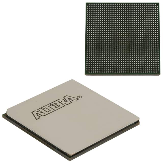
Lihat spesifikasi untuk detail produk.

5CGXFC9E6F35I7N
Product Overview
Category
The 5CGXFC9E6F35I7N belongs to the category of Field-Programmable Gate Arrays (FPGAs).
Use
FPGAs are integrated circuits that can be programmed after manufacturing. The 5CGXFC9E6F35I7N is specifically designed for high-performance applications that require complex digital logic functions.
Characteristics
- High-performance FPGA with advanced features
- Offers a large number of programmable logic elements
- Provides high-speed interfaces and connectivity options
- Supports various communication protocols
- Enables efficient power management
Package
The 5CGXFC9E6F35I7N comes in a compact package, which ensures easy integration into electronic systems.
Essence
The essence of the 5CGXFC9E6F35I7N lies in its ability to provide flexible and customizable digital logic functionality, allowing designers to implement complex algorithms and designs efficiently.
Packaging/Quantity
The 5CGXFC9E6F35I7N is typically packaged individually and is available in various quantities depending on the requirements of the project.
Specifications
- Logic Elements: 9,150
- Embedded Memory: 1,638 Kbits
- Maximum User I/Os: 622
- DSP Blocks: 144
- Clock Networks: 16
- Total RAM Bits: 2,621,440
- Maximum Operating Frequency: 350 MHz
- Voltage Range: 0.87V - 0.93V
- Package Type: F35
- Temperature Range: -40°C to +100°C
Detailed Pin Configuration
The detailed pin configuration of the 5CGXFC9E6F35I7N can be found in the manufacturer's datasheet. It provides information on the specific functions and connections of each pin.
Functional Features
- High-speed serial transceivers for data communication
- On-chip memory blocks for efficient data storage
- Dedicated digital signal processing (DSP) blocks for complex mathematical operations
- Flexible clock management resources for precise timing control
- Support for various communication protocols, such as PCIe, Ethernet, and USB
Advantages and Disadvantages
Advantages
- Flexibility: The 5CGXFC9E6F35I7N allows designers to implement custom logic functions, providing flexibility in system design.
- High Performance: With its advanced features and high-speed interfaces, the FPGA delivers excellent performance for demanding applications.
- Power Efficiency: The device incorporates power management techniques, enabling efficient utilization of resources and reducing power consumption.
Disadvantages
- Complexity: Programming and configuring FPGAs can be challenging, requiring specialized knowledge and expertise.
- Cost: FPGAs tend to be more expensive compared to other integrated circuits due to their programmable nature.
Working Principles
The 5CGXFC9E6F35I7N operates based on the principles of reconfigurable computing. It consists of an array of configurable logic elements interconnected through programmable routing resources. These logic elements can be programmed to perform desired digital logic functions, allowing for the implementation of complex algorithms and designs.
Detailed Application Field Plans
The 5CGXFC9E6F35I7N finds applications in various fields, including:
- Telecommunications: Used in base stations, routers, and network switches for high-speed data processing and communication.
- Aerospace and Defense: Employed in radar systems, avionics, and military communication equipment for their high-performance and flexibility.
- Industrial Automation: Utilized in control systems, robotics, and machine vision applications for real-time processing and control.
- Medical Devices: Integrated into medical imaging systems, patient monitoring devices, and diagnostic equipment for their computational capabilities.
- Automotive: Used in advanced driver-assistance systems (ADAS), infotainment systems, and engine control units (ECUs) for enhanced functionality.
Detailed and Complete Alternative Models
- 5CGXFC7D6F31C7N
- 5CGXFC9E7F31I7N
- 5CGXFC9E7F31C7N
- 5CGXFC9E7F35I7N
- 5CGXFC9E7F35C7N
These alternative models offer similar features and capabilities to the 5CGXFC9E6F35I7N, providing designers with options based on their specific requirements.
Note: The above information is subject to change. For the most accurate and up-to-date details, refer to the manufacturer's datasheet and product documentation.
Word Count: 550
Sebutkan 10 pertanyaan dan jawaban umum terkait penerapan 5CGXFC9E6F35I7N dalam solusi teknis
Sure! Here are 10 common questions and answers related to the application of 5CGXFC9E6F35I7N in technical solutions:
Q: What is the 5CGXFC9E6F35I7N FPGA used for? A: The 5CGXFC9E6F35I7N FPGA is commonly used for implementing complex digital logic designs in various technical solutions.
Q: What are some typical applications of the 5CGXFC9E6F35I7N FPGA? A: Some typical applications include telecommunications, industrial automation, automotive electronics, medical devices, and high-performance computing.
Q: What are the key features of the 5CGXFC9E6F35I7N FPGA? A: The key features include a large number of programmable logic elements, high-speed transceivers, embedded memory blocks, and support for various I/O standards.
Q: Can the 5CGXFC9E6F35I7N FPGA be reprogrammed? A: Yes, the 5CGXFC9E6F35I7N FPGA is reprogrammable, allowing for flexibility in design iterations and updates.
Q: How does the 5CGXFC9E6F35I7N FPGA handle high-speed data processing? A: The FPGA's high-speed transceivers enable it to handle high-speed data processing, making it suitable for applications requiring fast data transfer rates.
Q: Does the 5CGXFC9E6F35I7N FPGA have built-in memory? A: Yes, the 5CGXFC9E6F35I7N FPGA has embedded memory blocks that can be used for storing data or implementing memory-intensive functions.
Q: Can the 5CGXFC9E6F35I7N FPGA interface with other components or devices? A: Yes, the FPGA supports various I/O standards and can interface with other components or devices such as sensors, displays, or communication interfaces.
Q: What development tools are available for programming the 5CGXFC9E6F35I7N FPGA? A: The 5CGXFC9E6F35I7N FPGA can be programmed using popular development tools like Quartus Prime from Intel (formerly Altera).
Q: Are there any reference designs or application notes available for the 5CGXFC9E6F35I7N FPGA? A: Yes, the manufacturer provides reference designs and application notes that can help developers get started with the FPGA and implement specific functionalities.
Q: Where can I find technical support or documentation for the 5CGXFC9E6F35I7N FPGA? A: Technical support and documentation can be found on the manufacturer's website or by contacting their customer support team.

