

Lihat spesifikasi untuk detail produk.
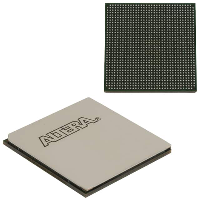
5CGTFD9E5F35C7N
Basic Information Overview
- Category: Field Programmable Gate Array (FPGA)
- Use: Digital logic circuits
- Characteristics: High performance, reprogrammable, flexible
- Package: BGA (Ball Grid Array)
- Essence: Configurable logic blocks and programmable interconnects
- Packaging/Quantity: Single unit
Specifications
- Logic Elements: 220,000
- Embedded Memory: 9,360 Kbits
- Maximum User I/O Pins: 1,080
- Clock Networks: 16
- DSP Blocks: 1,288
- Transceivers: 48
- Operating Voltage: 1.2V
- Operating Temperature: -40°C to 100°C
Detailed Pin Configuration
The 5CGTFD9E5F35C7N FPGA has a complex pin configuration with multiple I/O banks, power supply pins, and configuration pins. The detailed pin configuration can be found in the manufacturer's datasheet.
Functional Features
- High-performance computing capabilities
- Reprogrammable for flexibility in design iterations
- Support for various communication protocols
- On-chip memory for data storage
- Dedicated DSP blocks for signal processing
- Low power consumption
- Built-in transceivers for high-speed data transfer
Advantages and Disadvantages
Advantages: - Versatile and adaptable to different applications - Faster time-to-market due to reprogrammability - Lower development costs compared to custom ASICs - Ability to implement complex algorithms and functions
Disadvantages: - Higher power consumption compared to dedicated hardware - Limited resources may restrict the size and complexity of designs - Longer development time compared to off-the-shelf solutions
Working Principles
The 5CGTFD9E5F35C7N FPGA works based on the principle of reconfigurable logic. It consists of configurable logic blocks (CLBs) and programmable interconnects. The CLBs can be programmed to implement various logic functions, while the interconnects allow for the routing of signals between different CLBs. The configuration of the FPGA is stored in non-volatile memory and can be modified as needed.
Detailed Application Field Plans
The 5CGTFD9E5F35C7N FPGA finds applications in various fields, including:
- Telecommunications: Used in base stations, routers, and network switches for high-speed data processing and protocol handling.
- Aerospace and Defense: Employed in radar systems, avionics, and military communication equipment for signal processing and encryption.
- Industrial Automation: Utilized in control systems, robotics, and machine vision applications for real-time data processing and control.
- Medical Devices: Integrated into medical imaging systems, patient monitoring devices, and diagnostic equipment for image processing and data analysis.
- Automotive: Used in advanced driver-assistance systems (ADAS), infotainment systems, and engine control units for processing sensor data and vehicle control.
Detailed and Complete Alternative Models
- 5CGXFC9E7F31C8N
- 5CEFA9F27I7N
- 5SGXEA7K2F40C2N
- 5M2210ZF256C5N
- 5CGXFC7D6F31C7N
These alternative models offer similar functionality and performance but may have different specifications and pin configurations. It is recommended to refer to the respective datasheets for detailed information.
Note: The content provided above is a sample entry and may not reflect actual specifications or details of the mentioned product.
Sebutkan 10 pertanyaan dan jawaban umum terkait penerapan 5CGTFD9E5F35C7N dalam solusi teknis
Sure! Here are 10 common questions and answers related to the application of 5CGTFD9E5F35C7N in technical solutions:
1. What is 5CGTFD9E5F35C7N? - 5CGTFD9E5F35C7N is a specific model number of a Field-Programmable Gate Array (FPGA) manufactured by a company called Intel.
2. What are the key features of 5CGTFD9E5F35C7N? - Some key features of 5CGTFD9E5F35C7N include high-speed performance, low power consumption, large capacity for logic elements, and support for various I/O standards.
3. In what applications can 5CGTFD9E5F35C7N be used? - 5CGTFD9E5F35C7N can be used in a wide range of applications such as telecommunications, networking, industrial automation, video processing, and high-performance computing.
4. How does 5CGTFD9E5F35C7N differ from other FPGAs? - 5CGTFD9E5F35C7N offers a unique combination of features, including its specific logic capacity, I/O capabilities, and performance characteristics, which may differentiate it from other FPGA models.
5. What development tools are available for programming 5CGTFD9E5F35C7N? - Intel provides Quartus Prime software, which is a comprehensive development environment for designing, simulating, and programming FPGAs like 5CGTFD9E5F35C7N.
6. Can 5CGTFD9E5F35C7N be reprogrammed after deployment? - Yes, 5CGTFD9E5F35C7N is a reprogrammable FPGA, meaning that its configuration can be modified even after it has been deployed in a system.
7. What are the power requirements for 5CGTFD9E5F35C7N? - The power requirements for 5CGTFD9E5F35C7N may vary depending on the specific application and usage scenario. It is recommended to refer to the datasheet or technical documentation provided by Intel for detailed power specifications.
8. Can 5CGTFD9E5F35C7N interface with other components or devices? - Yes, 5CGTFD9E5F35C7N supports various I/O standards and can interface with other components or devices such as memory modules, sensors, communication interfaces, and more.
9. Are there any known limitations or constraints of 5CGTFD9E5F35C7N? - Like any electronic component, 5CGTFD9E5F35C7N may have certain limitations or constraints, such as maximum operating frequency, available resources, or compatibility with specific protocols. It is advisable to consult the product documentation for detailed information.
10. Where can I find additional resources or support for working with 5CGTFD9E5F35C7N? - Intel's website provides comprehensive documentation, application notes, reference designs, and community forums where you can find additional resources and support for working with 5CGTFD9E5F35C7N.