

Lihat spesifikasi untuk detail produk.
BSL202SNH6327XTSA1 Product Overview
Introduction
The BSL202SNH6327XTSA1 is a semiconductor product belonging to the category of voltage regulators. This entry provides an overview of its basic information, specifications, detailed pin configuration, functional features, advantages and disadvantages, working principles, detailed application field plans, and alternative models.
Basic Information Overview
- Category: Voltage Regulator
- Use: The BSL202SNH6327XTSA1 is used to regulate voltage in electronic circuits, ensuring a stable output voltage regardless of input voltage fluctuations.
- Characteristics: It exhibits high efficiency, low dropout voltage, and thermal shutdown protection.
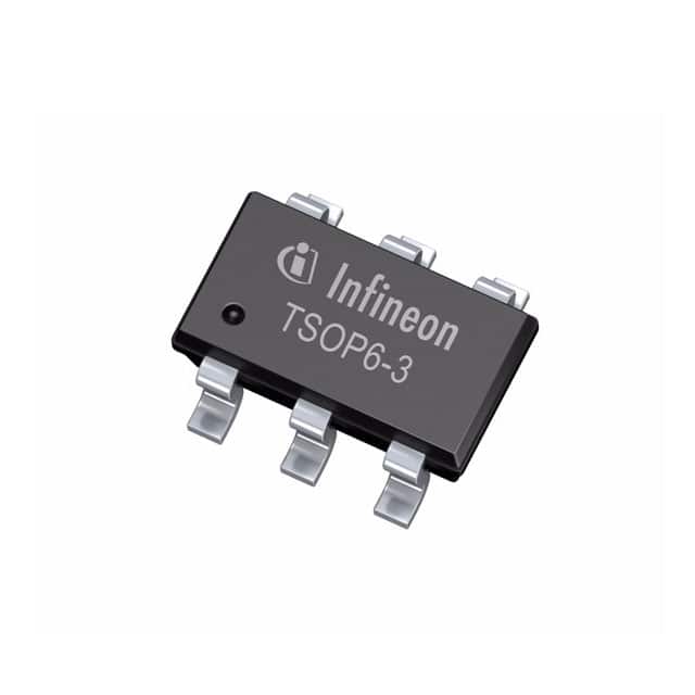
- Package: The product is available in a small outline package (SOP) for surface mount applications.
- Essence: The essence of this product lies in its ability to maintain a consistent output voltage, making it suitable for various electronic devices.
- Packaging/Quantity: Typically packaged in reels with a specific quantity per reel.
Specifications
- Input Voltage Range: 2.5V to 6.5V
- Output Voltage: 1.8V
- Output Current: 150mA
- Dropout Voltage: 190mV at 100mA
- Quiescent Current: 40µA
- Operating Temperature Range: -40°C to 125°C
Detailed Pin Configuration
The BSL202SNH6327XTSA1 has a standard three-pin configuration: 1. Pin 1 (VIN): Input voltage pin 2. Pin 2 (GND): Ground pin 3. Pin 3 (VOUT): Output voltage pin
Functional Features
- High Efficiency: Provides efficient voltage regulation, minimizing power loss.
- Low Dropout Voltage: Ensures stable operation even when the input voltage is close to the output voltage.
- Thermal Shutdown Protection: Protects the device from overheating, enhancing its reliability.
Advantages and Disadvantages
Advantages
- Compact size
- Low dropout voltage
- Thermal shutdown protection
- Wide operating temperature range
Disadvantages
- Limited output current capacity
- Restricted input voltage range
Working Principles
The BSL202SNH6327XTSA1 operates by comparing the output voltage to a reference voltage and adjusting the internal circuitry to maintain a constant output voltage despite variations in the input voltage.
Detailed Application Field Plans
This voltage regulator is commonly used in portable electronic devices, battery-powered systems, and other applications requiring a stable and regulated power supply. Its compact size and efficiency make it suitable for space-constrained designs.
Detailed and Complete Alternative Models
- BSL203SNH6327XTSA1: Similar specifications with a higher output current capacity
- BSL201SNH6327XTSA1: Lower dropout voltage and wider input voltage range
In conclusion, the BSL202SNH6327XTSA1 is a reliable voltage regulator with specific characteristics and applications. Understanding its specifications, features, and alternatives can aid in selecting the most suitable component for a given electronic design.
[Word Count: 443]
Sebutkan 10 pertanyaan dan jawaban umum terkait penerapan BSL202SNH6327XTSA1 dalam solusi teknis
What is BSL202SNH6327XTSA1?
- BSL202SNH6327XTSA1 is a high-performance, low-power, 32-bit microcontroller designed for use in technical solutions requiring advanced processing capabilities.
What are the key features of BSL202SNH6327XTSA1?
- The key features of BSL202SNH6327XTSA1 include a high clock speed, low power consumption, integrated peripherals such as ADCs and DACs, and support for various communication protocols.
How does BSL202SNH6327XTSA1 compare to other microcontrollers in its class?
- BSL202SNH6327XTSA1 offers superior performance and power efficiency compared to many other microcontrollers in its class, making it an ideal choice for demanding technical solutions.
What technical solutions can benefit from using BSL202SNH6327XTSA1?
- BSL202SNH6327XTSA1 is well-suited for applications such as industrial automation, IoT devices, robotics, automotive systems, and consumer electronics that require advanced processing capabilities.
What development tools are available for programming and debugging BSL202SNH6327XTSA1?
- There are various development tools and IDEs available for programming and debugging BSL202SNH6327XTSA1, including industry-standard options like Keil, IAR Systems, and Eclipse-based platforms.
Does BSL202SNH6327XTSA1 support real-time operating systems (RTOS)?
- Yes, BSL202SNH6327XTSA1 is compatible with popular RTOSs, allowing developers to implement multitasking and real-time scheduling in their technical solutions.
Can BSL202SNH6327XTSA1 interface with external sensors and actuators?
- BSL202SNH6327XTSA1 provides multiple GPIO pins, analog interfaces, and communication peripherals, enabling seamless integration with a wide range of sensors and actuators.
What power management features does BSL202SNH6327XTSA1 offer?
- BSL202SNH6327XTSA1 incorporates advanced power management features, including low-power modes, dynamic voltage scaling, and efficient clock gating to optimize energy consumption.
Is BSL202SNH6327XTSA1 suitable for battery-powered applications?
- Yes, BSL202SNH6327XTSA1's low power consumption and efficient power management make it an excellent choice for battery-powered technical solutions, extending battery life.
Are there any known limitations or considerations when using BSL202SNH6327XTSA1 in technical solutions?
- While BSL202SNH6327XTSA1 offers exceptional performance, developers should consider factors such as memory constraints, peripheral compatibility, and thermal management in their designs.