

Lihat spesifikasi untuk detail produk.
IDT5V995PFGI8
Product Overview
Category
The IDT5V995PFGI8 belongs to the category of integrated circuits (ICs).
Use
This IC is commonly used in electronic devices for signal switching and routing applications.
Characteristics
- High-speed performance
- Low power consumption
- Wide operating voltage range
- Small form factor
Package
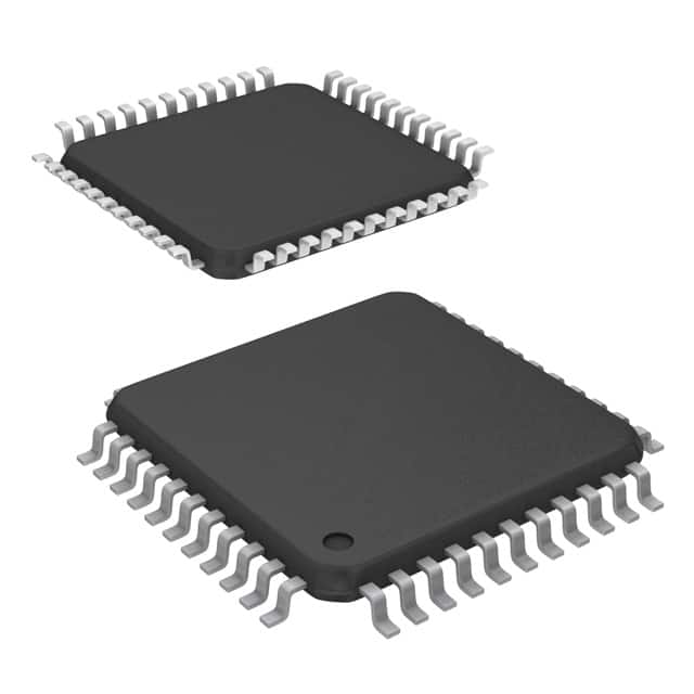
The IDT5V995PFGI8 is available in a compact and industry-standard package, such as a 48-pin TQFP (Thin Quad Flat Package).
Essence
The essence of the IDT5V995PFGI8 lies in its ability to efficiently switch and route signals within electronic systems.
Packaging/Quantity
The IC is typically packaged in reels or tubes, with a quantity of 250 units per reel/tube.
Specifications
- Supply Voltage: 2.7V to 3.6V
- Operating Temperature Range: -40°C to +85°C
- Input/Output Logic Levels: CMOS/TTL compatible
- Switching Frequency: Up to 100 MHz
- On-Resistance: 4Ω (typical)
- Number of Channels: 10
Detailed Pin Configuration
The IDT5V995PFGI8 features a 48-pin TQFP package with the following pin configuration:
- VCC
- GND
- IN0
- OUT0
- IN1
- OUT1
- IN2
- OUT2
- IN3
- OUT3
- IN4
- OUT4
- IN5
- OUT5
- IN6
- OUT6
- IN7
- OUT7
- IN8
- OUT8
- IN9
- OUT9
- OE (Output Enable)
- SEL (Channel Select) 25-48. NC (No Connection)
Functional Features
The IDT5V995PFGI8 offers the following functional features:
- 10-channel bidirectional signal switching
- Independent channel selection
- Output enable control
- Low power consumption in standby mode
- Fast switching speed
- Wide operating voltage range
Advantages and Disadvantages
Advantages
- High-speed performance enables efficient signal routing
- Low power consumption helps conserve energy
- Wide operating voltage range allows compatibility with various systems
- Compact package size facilitates integration into space-constrained designs
Disadvantages
- Limited number of channels may not be suitable for applications requiring a higher channel count
- On-resistance may introduce some signal attenuation
Working Principles
The IDT5V995PFGI8 operates based on CMOS technology, utilizing MOSFET transistors to switch signals between input and output channels. The control signals provided through the channel select pins determine which channel is active, while the output enable pin enables or disables the output stage.
Detailed Application Field Plans
The IDT5V995PFGI8 finds application in various fields, including but not limited to:
- Communication systems
- Data acquisition systems
- Test and measurement equipment
- Audio/video routing systems
- Industrial automation
Detailed and Complete Alternative Models
- Texas Instruments SN74CBT3257: This IC offers similar functionality with a different pin configuration.
- NXP 74LVC245: Provides bidirectional signal switching with a larger number of channels.
- Maxim Integrated MAX4544: Offers high-speed signal routing capabilities with low power consumption.
These alternative models can be considered based on specific requirements and design constraints.
In conclusion, the IDT5V995PFGI8 is a versatile integrated circuit that excels in signal switching and routing applications. Its high-speed performance, low power consumption, and compact package make it suitable for various electronic systems. However, designers should consider the limited number of channels and potential signal attenuation when selecting this IC.
Sebutkan 10 pertanyaan dan jawaban umum terkait penerapan IDT5V995PFGI8 dalam solusi teknis
Sure! Here are 10 common questions and answers related to the application of IDT5V995PFGI8 in technical solutions:
Q: What is IDT5V995PFGI8? A: IDT5V995PFGI8 is a high-performance clock generator and fanout buffer designed for use in various technical solutions.
Q: What are the key features of IDT5V995PFGI8? A: Some key features include low output skew, low phase noise, multiple outputs, wide frequency range, and compatibility with various input types.
Q: What is the purpose of using IDT5V995PFGI8 in technical solutions? A: IDT5V995PFGI8 is used to generate and distribute precise clock signals, ensuring synchronization and timing accuracy in complex systems.
Q: What is the frequency range supported by IDT5V995PFGI8? A: IDT5V995PFGI8 supports a wide frequency range, typically from a few megahertz up to several hundred megahertz.
Q: Can IDT5V995PFGI8 be used with different input signal types? A: Yes, IDT5V995PFGI8 is compatible with various input signal types, including LVCMOS, LVTTL, and LVPECL.
Q: How many outputs does IDT5V995PFGI8 have? A: IDT5V995PFGI8 has multiple outputs, typically ranging from 4 to 12, depending on the specific variant.
Q: Does IDT5V995PFGI8 provide any output skew adjustment options? A: No, IDT5V995PFGI8 does not have built-in output skew adjustment capabilities.
Q: What is the power supply voltage range for IDT5V995PFGI8? A: The power supply voltage range for IDT5V995PFGI8 is typically between 3.3V and 5V.
Q: Can IDT5V995PFGI8 be used in high-speed data communication applications? A: Yes, IDT5V995PFGI8 can be used in high-speed data communication applications that require precise clock synchronization.
Q: Are there any specific application notes or reference designs available for IDT5V995PFGI8? A: Yes, the manufacturer provides application notes and reference designs to help users implement IDT5V995PFGI8 effectively in their technical solutions.
Please note that the answers provided here are general and may vary depending on the specific requirements and use cases of your technical solution.