

Lihat spesifikasi untuk detail produk.
IDT5V991A-2JG8
Product Overview
Category
The IDT5V991A-2JG8 belongs to the category of integrated circuits (ICs).
Use
This product is commonly used in electronic devices for signal conditioning and level shifting applications.
Characteristics
- The IDT5V991A-2JG8 is a high-performance voltage level translator.
- It operates at a wide range of supply voltages, making it suitable for various applications.
- This IC provides bidirectional voltage translation between different logic levels.
- It offers low power consumption and high-speed performance.
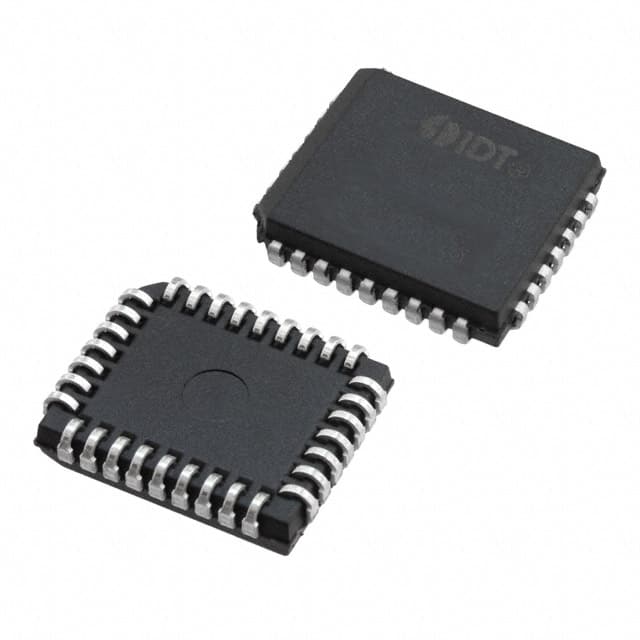
Package
The IDT5V991A-2JG8 is available in a small form factor package, such as a 20-pin TSSOP (Thin Shrink Small Outline Package).
Essence
The essence of this product lies in its ability to seamlessly translate voltage levels between different logic families, enabling smooth communication between incompatible devices.
Packaging/Quantity
The IDT5V991A-2JG8 is typically packaged in reels or tubes, with a quantity of 250 units per reel/tube.
Specifications
- Supply Voltage Range: 1.2V to 3.6V
- Logic Voltage Levels: 1.8V, 2.5V, 3.3V
- Operating Temperature Range: -40°C to +85°C
- Input/Output Compatibility: CMOS, TTL, LVCMOS, LVTTL
- Maximum Data Rate: 100 Mbps
- Propagation Delay: 4 ns (typical)
Detailed Pin Configuration
The IDT5V991A-2JG8 has a total of 20 pins. Here is the detailed pin configuration:
- VCCA - Power supply voltage for side A
- GND - Ground
- A1 - Side A input/output pin 1
- A2 - Side A input/output pin 2
- A3 - Side A input/output pin 3
- A4 - Side A input/output pin 4
- A5 - Side A input/output pin 5
- OE - Output enable
- B5 - Side B input/output pin 5
- B4 - Side B input/output pin 4
- B3 - Side B input/output pin 3
- B2 - Side B input/output pin 2
- B1 - Side B input/output pin 1
- GND - Ground
- VCCB - Power supply voltage for side B
- B6 - Side B input/output pin 6
- B7 - Side B input/output pin 7
- B8 - Side B input/output pin 8
- B9 - Side B input/output pin 9
- B10 - Side B input/output pin 10
Functional Features
- Bidirectional voltage level translation between different logic families.
- Automatic direction sensing and control.
- Low power consumption.
- High-speed operation.
- ESD protection on all pins.
Advantages and Disadvantages
Advantages
- Wide supply voltage range allows compatibility with various systems.
- High-speed performance enables efficient data transmission.
- Automatic direction sensing simplifies system design.
- ESD protection ensures robustness against electrostatic discharge.
Disadvantages
- Limited maximum data rate compared to some other voltage level translators.
- Availability in a specific package may limit its use in certain applications.
Working Principles
The IDT5V991A-2JG8 utilizes a combination of level shifting circuitry and automatic direction sensing to translate voltage levels between different logic families. It detects the direction of data flow and adjusts the voltage levels accordingly, ensuring seamless communication between devices operating at different logic voltages.
Detailed Application Field Plans
The IDT5V991A-2JG8 finds applications in various fields, including:
- Communication systems: Facilitating voltage level translation between different components in communication systems, such as microcontrollers, sensors, and display modules.
- Industrial automation: Enabling compatibility between different logic families in industrial automation equipment, such as PLCs (Programmable Logic Controllers) and motor control systems.
- Consumer electronics: Supporting voltage level translation in consumer electronic devices, including smartphones, tablets, and gaming consoles.
- Automotive electronics: Ensuring smooth communication between different components in automotive systems, such as infotainment systems, instrument clusters, and ECU (Engine Control Unit).
Detailed and Complete Alternative Models
- SN74LVC1T45: A single-bit voltage level translator with similar characteristics and package options.
- PCA9306: A bidirectional I2C-bus voltage level translator suitable for low-speed applications.
- TXB0108: An 8
Sebutkan 10 pertanyaan dan jawaban umum terkait penerapan IDT5V991A-2JG8 dalam solusi teknis
Sure! Here are 10 common questions and answers related to the application of IDT5V991A-2JG8 in technical solutions:
Q: What is the IDT5V991A-2JG8? A: The IDT5V991A-2JG8 is a high-performance video clock generator and jitter attenuator IC.
Q: What are the key features of the IDT5V991A-2JG8? A: The key features include multiple input options, low jitter output clocks, programmable PLL, and support for various video standards.
Q: What are the typical applications of the IDT5V991A-2JG8? A: It is commonly used in video distribution systems, video surveillance, broadcast equipment, and other applications requiring precise video clock generation.
Q: How does the IDT5V991A-2JG8 handle jitter attenuation? A: The IC uses a phase-locked loop (PLL) to reduce the amount of jitter in the input clock signal, resulting in a cleaner and more stable output clock.
Q: Can the IDT5V991A-2JG8 generate multiple output clocks? A: Yes, it can generate up to four independent output clocks with different frequencies and formats.
Q: What video standards are supported by the IDT5V991A-2JG8? A: It supports various video standards such as NTSC, PAL, SECAM, and HDTV formats like 720p, 1080i, and 1080p.
Q: Is the IDT5V991A-2JG8 compatible with different input signal types? A: Yes, it supports a wide range of input signal types, including analog composite video, S-video, and component video.
Q: Can the IDT5V991A-2JG8 be programmed for specific clock frequencies? A: Yes, it offers programmable frequency dividers and PLL settings, allowing users to configure the output clocks to their desired frequencies.
Q: Does the IDT5V991A-2JG8 require any external components for operation? A: It requires a few external passive components like resistors and capacitors for proper operation and stability.
Q: What is the power supply requirement for the IDT5V991A-2JG8? A: The IC operates on a single 3.3V power supply, making it compatible with standard digital logic levels.
Please note that these answers are general and may vary depending on the specific application and requirements.