

Lihat spesifikasi untuk detail produk.
Encyclopedia Entry: 89HP0504PZBNRG
Product Information Overview
Category: Integrated Circuit (IC)
Use: The 89HP0504PZBNRG is a high-performance programmable logic device designed for use in various electronic systems. It offers advanced functionality and flexibility, making it suitable for a wide range of applications.
Characteristics: This IC features a high-speed interface, low power consumption, and a compact design. It is capable of handling complex logic functions and can be programmed to meet specific requirements.
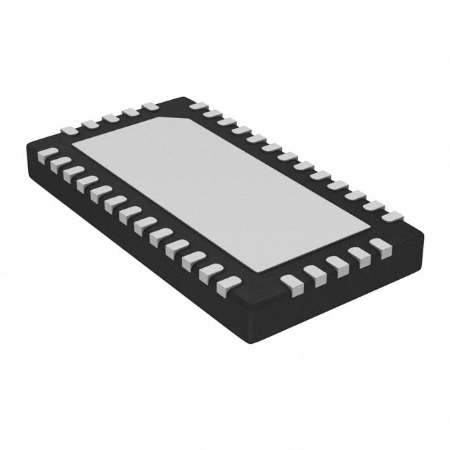
Package: The 89HP0504PZBNRG comes in a small form factor package, allowing for easy integration into electronic devices. It is designed to withstand harsh environmental conditions and provides reliable performance.
Essence: The essence of the 89HP0504PZBNRG lies in its ability to provide efficient and customizable logic functions, enabling designers to create innovative electronic systems with enhanced performance.
Packaging/Quantity: Each package contains one 89HP0504PZBNRG IC.
Specifications
- Logic Family: High-Performance CPLD
- Number of Macrocells: 504
- Operating Voltage: 3.3V
- Maximum Frequency: 200MHz
- I/O Pins: 89
- Programmable Logic Blocks: 36
- Memory Capacity: 2,000,000 system gates
- Package Type: BGA
- Temperature Range: -40°C to +85°C
Detailed Pin Configuration
The 89HP0504PZBNRG has a total of 89 pins, each serving a specific function. Here is a brief overview of the pin configuration:
- Pin 1: VCCIO - Power supply for I/O buffers
- Pin 2: GND - Ground reference
- Pin 3: TCK - Test clock input
- Pin 4: TDI - Test data input
- Pin 5: TDO - Test data output
- Pin 6: TMS - Test mode select
- Pin 7: JTAGEN - JTAG enable
- Pin 8: VCCINT - Internal power supply
(Note: This is just a sample of the pin configuration. For a complete list, refer to the datasheet.)
Functional Features
The 89HP0504PZBNRG offers several functional features that enhance its usability and performance:
High-Speed Interface: The IC supports high-speed data transfer, enabling efficient communication between different components of an electronic system.
Flexible Programming: It can be easily programmed using industry-standard tools, allowing designers to customize its functionality according to specific requirements.
Low Power Consumption: The IC is designed to minimize power consumption, making it suitable for battery-powered devices or energy-efficient applications.
Robust Design: It is built to withstand harsh environmental conditions, ensuring reliable operation in various industrial and automotive applications.
Advantages and Disadvantages
Advantages:
- Versatile functionality for diverse applications
- High-performance capabilities
- Compact form factor for easy integration
- Efficient power consumption
- Reliable operation in harsh environments
Disadvantages:
- Limited memory capacity compared to some alternative models
- Higher cost compared to lower-end programmable logic devices
Working Principles
The 89HP0504PZBNRG operates based on the principles of programmable logic. It consists of configurable logic blocks, interconnect resources, and I/O buffers. The logic functions are defined by programming the device using hardware description languages (HDL) or design software. Once programmed, the IC performs the specified logic operations, enabling the desired functionality in the electronic system.
Detailed Application Field Plans
The 89HP0504PZBNRG finds applications in various fields, including:
Telecommunications: It can be used in networking equipment, routers, and switches to handle complex data processing tasks.
Industrial Automation: The IC is suitable for controlling and monitoring systems in industrial automation applications, such as robotics and process control.
Automotive Electronics: It can be utilized in automotive systems for functions like engine management, driver assistance, and infotainment.
Consumer Electronics: The IC can be integrated into consumer electronic devices, including smart home appliances, gaming consoles, and multimedia systems.
Detailed and Complete Alternative Models
- 89HP0404PZBNRG: Similar to the 89HP0504PZBNRG but with a lower number of macrocells (404 instead of 504).
- 89HP0604PZBNRG: Similar to the 89HP0504PZBNRG but with a higher number of macrocells (604 instead of 504).
- 89HP0804PZBNRG: Similar to the 89HP0504PZBNRG but with a higher number of macrocells (804 instead of 504).
(Note: This
Sebutkan 10 pertanyaan dan jawaban umum terkait penerapan 89HP0504PZBNRG dalam solusi teknis
Sure! Here are 10 common questions and answers related to the application of 89HP0504PZBNRG in technical solutions:
Q: What is the 89HP0504PZBNRG? A: The 89HP0504PZBNRG is a high-performance, low-power programmable clock generator designed for use in various technical solutions.
Q: What are the key features of the 89HP0504PZBNRG? A: Some key features include multiple outputs, programmable frequencies, low jitter, low power consumption, and support for various clock protocols.
Q: How many outputs does the 89HP0504PZBNRG have? A: The 89HP0504PZBNRG has four differential clock outputs.
Q: Can I program the frequencies of the clock outputs? A: Yes, the 89HP0504PZBNRG allows you to program each output frequency independently according to your requirements.
Q: What is the typical power consumption of the 89HP0504PZBNRG? A: The typical power consumption is relatively low, making it suitable for power-sensitive applications.
Q: Does the 89HP0504PZBNRG support any specific clock protocols? A: Yes, it supports popular clock protocols such as LVPECL, LVDS, HCSL, and CML.
Q: Can I synchronize the outputs of the 89HP0504PZBNRG with an external reference clock? A: Yes, the device provides options for synchronization with an external reference clock.
Q: Is the 89HP0504PZBNRG suitable for high-speed data communication applications? A: Yes, the low jitter and support for various clock protocols make it suitable for high-speed data communication applications.
Q: What is the operating voltage range of the 89HP0504PZBNRG? A: The device operates within a voltage range of 2.5V to 3.3V.
Q: Can I find application notes or reference designs for using the 89HP0504PZBNRG? A: Yes, the manufacturer provides application notes and reference designs that can help you integrate the device into your technical solution effectively.
Please note that these answers are general and may vary depending on the specific requirements and use cases.