

Lihat spesifikasi untuk detail produk.
Encyclopedia Entry: 74FCT162827ATPVG8
Product Information Overview
- Category: Integrated Circuit (IC)
- Use: Logic Level Translator
- Characteristics: High-speed, low-power consumption
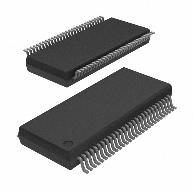
- Package: TSSOP (Thin Shrink Small Outline Package)
- Essence: Translates logic levels between different voltage domains
- Packaging/Quantity: Tape and Reel, 2500 units per reel
Specifications
- Logic Family: FCT
- Number of Channels: 16
- Input Voltage Range: 2.0V to 5.5V
- Output Voltage Range: 2.0V to 5.5V
- Propagation Delay: 3.5 ns (typical)
- Operating Temperature Range: -40°C to +85°C
Detailed Pin Configuration
The 74FCT162827ATPVG8 IC has a total of 56 pins, which are organized as follows:
- Pins 1-8: Channel A Inputs (A0-A7)
- Pins 9-16: Channel B Inputs (B0-B7)
- Pins 17-24: Channel A Outputs (QA0-QA7)
- Pins 25-32: Channel B Outputs (QB0-QB7)
- Pins 33-40: Channel Enable Inputs (GAB0-GAB7)
- Pins 41-48: Channel Output Enable Inputs (OEAB0-OEAB7)
- Pins 49-56: Ground and Power Supply Pins (GND, VCC)
Functional Features
- Logic level translation between two voltage domains
- Bidirectional data flow capability
- Non-inverting outputs
- High-speed operation
- Low power consumption
- ESD protection on all inputs and outputs
Advantages and Disadvantages
Advantages: - High-speed operation allows for efficient data transfer - Low power consumption helps in reducing overall system energy usage - Bidirectional data flow capability simplifies circuit design - ESD protection ensures reliability in harsh environments
Disadvantages: - Limited voltage range (2.0V to 5.5V) may not be suitable for all applications - TSSOP package may require careful handling during assembly
Working Principles
The 74FCT162827ATPVG8 is a logic level translator IC that enables communication between two different voltage domains. It operates by receiving input signals from one voltage domain and translating them to the appropriate logic levels compatible with the other voltage domain. The bidirectional data flow capability allows for seamless communication in both directions.
The IC utilizes non-inverting outputs, ensuring that the translated signals maintain their original logic state. With high-speed operation and low power consumption, it provides efficient and reliable logic level translation for various applications.
Detailed Application Field Plans
The 74FCT162827ATPVG8 IC finds application in various fields where logic level translation is required. Some of the potential application areas include:
- Microcontroller interfacing with different voltage peripherals
- Communication systems involving multiple voltage domains
- Industrial automation and control systems
- Automotive electronics
- Consumer electronics devices
Detailed and Complete Alternative Models
74LVC162827A: Low Voltage CMOS Logic Level Translator
- Logic Family: LVC
- Input/Output Voltage Range: 1.65V to 5.5V
- Propagation Delay: 6 ns (typical)
- Package: TSSOP
SN74AVC162827DGGR: Advanced CMOS Logic Level Translator
- Logic Family: AVC
- Input/Output Voltage Range: 1.2V to 3.6V
- Propagation Delay: 4 ns (typical)
- Package: TSSOP
NC7SZ125P5X: TinyLogic UHS Buffer with 3-State Output
- Logic Family: TinyLogic UHS
- Input/Output Voltage Range: 0.9V to 3.6V
- Propagation Delay: 2.5 ns (typical)
- Package: SC-70
These alternative models offer different voltage ranges, propagation delays, and package options, providing flexibility for various design requirements.
In conclusion, the 74FCT162827ATPVG8 is a high-speed logic level translator IC that enables seamless communication between different voltage domains. With its bidirectional data flow capability, low power consumption, and ESD protection, it finds applications in diverse fields such as microcontroller interfacing, communication systems, industrial automation, automotive electronics, and consumer electronics devices.
Sebutkan 10 pertanyaan dan jawaban umum terkait penerapan 74FCT162827ATPVG8 dalam solusi teknis
Sure! Here are 10 common questions and answers related to the application of 74FCT162827ATPVG8 in technical solutions:
Q: What is the 74FCT162827ATPVG8? A: The 74FCT162827ATPVG8 is a high-speed, low-power 20-bit buffer/line driver with 3-state outputs.
Q: What is the operating voltage range for this device? A: The operating voltage range for the 74FCT162827ATPVG8 is typically between 4.5V and 5.5V.
Q: What is the maximum data rate supported by this device? A: The 74FCT162827ATPVG8 can support data rates up to 200 MHz.
Q: Can this device be used as a bidirectional buffer? A: Yes, the 74FCT162827ATPVG8 can be used as a bidirectional buffer, allowing data to flow in both directions.
Q: What is the output drive strength of this device? A: The 74FCT162827ATPVG8 has a typical output drive strength of ±24 mA.
Q: Does this device have internal pull-up or pull-down resistors? A: No, the 74FCT162827ATPVG8 does not have internal pull-up or pull-down resistors.
Q: Can this device be cascaded to increase the number of buffered outputs? A: Yes, multiple 74FCT162827ATPVG8 devices can be cascaded together to increase the number of buffered outputs.
Q: Is this device compatible with TTL and CMOS logic levels? A: Yes, the 74FCT162827ATPVG8 is compatible with both TTL and CMOS logic levels.
Q: What is the power consumption of this device? A: The power consumption of the 74FCT162827ATPVG8 is typically around 50 mW.
Q: Can this device be used in high-speed data communication applications? A: Yes, the 74FCT162827ATPVG8 is suitable for high-speed data communication applications such as data buses, memory interfaces, and clock distribution.
Please note that these answers are general and may vary depending on specific application requirements and datasheet specifications.