

Lihat spesifikasi untuk detail produk.
XR68C681P
Product Overview
- Category: Integrated Circuit (IC)
- Use: XR68C681P is a versatile IC used for various applications in electronic devices.
- Characteristics: The XR68C681P offers high performance and reliability, with advanced features that make it suitable for a wide range of applications.
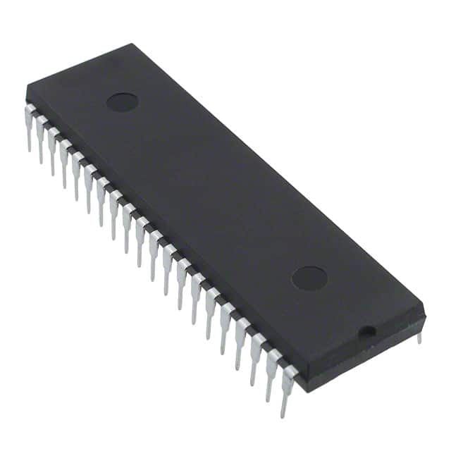
- Package: The XR68C681P comes in a compact and durable package, ensuring easy installation and protection against external factors.
- Essence: This IC is designed to provide efficient and accurate signal processing, enabling seamless operation of electronic devices.
- Packaging/Quantity: The XR68C681P is typically packaged in reels or tubes, with varying quantities depending on the manufacturer's specifications.
Specifications
The XR68C681P has the following specifications:
- Input Voltage Range: 3.3V - 5V
- Operating Temperature Range: -40°C to +85°C
- Maximum Clock Frequency: 20 MHz
- Number of Pins: 28
- Power Consumption: Low power consumption for energy-efficient operation
- Communication Interface: Serial communication interface for easy integration with other components
Detailed Pin Configuration
The XR68C681P has a total of 28 pins, each serving a specific function. The pin configuration is as follows:
- VCC: Power supply voltage input
- GND: Ground reference
- RESET: Reset signal input
- CLK: Clock signal input
- DATA_IN: Data input
- DATA_OUT: Data output
- A0-A3: Address inputs
- CS: Chip select input
- INT: Interrupt output
- RD: Read control input
- WR: Write control input
- D0-D7: Data bus lines
Functional Features
The XR68C681P offers the following functional features:
- High-speed data processing
- Flexible address and data bus configuration
- Interrupt capability for efficient event handling
- Easy integration with other components through a serial communication interface
- Low power consumption for energy-efficient operation
Advantages and Disadvantages
Advantages of using XR68C681P:
- Versatile and suitable for various applications
- High performance and reliability
- Efficient signal processing
- Easy integration with other components
- Low power consumption
Disadvantages of using XR68C681P:
- Limited clock frequency compared to some other ICs in the market
- Availability may vary depending on the manufacturer's stock
Working Principles
The XR68C681P operates based on the principles of digital signal processing. It receives input signals, processes them using its internal circuitry, and produces output signals according to the programmed logic. The IC utilizes a clock signal to synchronize its operations and communicates with other components through a serial interface.
Detailed Application Field Plans
The XR68C681P can be used in various electronic devices and applications, including but not limited to:
- Industrial automation systems
- Consumer electronics
- Communication equipment
- Automotive electronics
- Medical devices
- Robotics
- Internet of Things (IoT) devices
Detailed and Complete Alternative Models
Some alternative models that offer similar functionality to XR68C681P are:
- XR68C682P
- XR68C683P
- XR68C684P
- XR68C685P
These alternative models provide comparable features and can be considered as substitutes for XR68C681P based on specific requirements and availability.
Note: The above information is subject to change based on the manufacturer's updates and revisions.
Sebutkan 10 pertanyaan dan jawaban umum terkait penerapan XR68C681P dalam solusi teknis
Sure! Here are 10 common questions and answers related to the application of XR68C681P in technical solutions:
Q: What is XR68C681P? A: XR68C681P is a UART (Universal Asynchronous Receiver Transmitter) chip commonly used for serial communication in technical solutions.
Q: What is the operating voltage range of XR68C681P? A: The operating voltage range of XR68C681P is typically between 4.5V and 5.5V.
Q: Can XR68C681P be used with both TTL and CMOS logic levels? A: Yes, XR68C681P is compatible with both TTL (Transistor-Transistor Logic) and CMOS (Complementary Metal-Oxide-Semiconductor) logic levels.
Q: What is the maximum baud rate supported by XR68C681P? A: XR68C681P supports a maximum baud rate of 115,200 bits per second.
Q: Does XR68C681P have built-in FIFO buffers? A: Yes, XR68C681P has built-in 16-byte transmit and receive FIFO (First-In-First-Out) buffers.
Q: Can XR68C681P be used for full-duplex communication? A: Yes, XR68C681P supports full-duplex communication, allowing simultaneous transmission and reception of data.
Q: Is XR68C681P compatible with RS-232 standard? A: No, XR68C681P is not directly compatible with RS-232 standard. However, it can be used with level shifters or RS-232 transceivers for RS-232 communication.
Q: What is the power consumption of XR68C681P? A: The power consumption of XR68C681P is typically around 10mA during active operation.
Q: Can XR68C681P be used in battery-powered applications? A: Yes, XR68C681P's low power consumption makes it suitable for battery-powered applications.
Q: Are there any application notes or reference designs available for XR68C681P? A: Yes, the manufacturer provides application notes and reference designs that can help in implementing XR68C681P in various technical solutions.
Please note that the answers provided here are general and may vary depending on specific use cases and requirements. It is always recommended to refer to the datasheet and documentation provided by the manufacturer for accurate information.