

Lihat spesifikasi untuk detail produk.
PI7C8150ANDE
Product Overview
- Category: Integrated Circuit
- Use: Signal Switching and Multiplexing
- Characteristics: High-speed, low-power, compact size
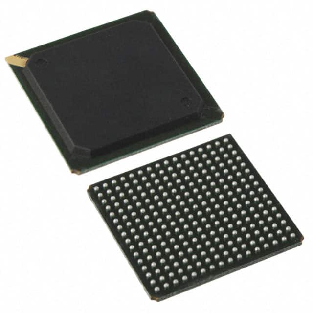
- Package: 48-pin QFN (Quad Flat No-Lead)
- Essence: A versatile signal switch for various applications
- Packaging/Quantity: Tape and Reel, 2500 units per reel
Specifications
- Supply Voltage: 3.3V
- Operating Temperature Range: -40°C to +85°C
- Input/Output Voltage Range: 0V to VCC
- Maximum Input Current: ±10mA
- Maximum Output Current: ±32mA
- Bandwidth: 1.5GHz
- On-Resistance: 2Ω
- Off-Isolation: -30dB
- Crosstalk: -35dB
- ESD Protection: >4kV (Human Body Model)
Pin Configuration
The PI7C8150ANDE has a total of 48 pins. The pin configuration is as follows:
- VCC
- GND
- IN1
- OUT1
- IN2
- OUT2
- IN3
- OUT3
- IN4
- OUT4
- IN5
- OUT5
- IN6
- OUT6
- IN7
- OUT7
- IN8
- OUT8
- IN9
- OUT9
- IN10
- OUT10
- IN11
- OUT11
- IN12
- OUT12
- IN13
- OUT13
- IN14
- OUT14
- IN15
- OUT15
- IN16
- OUT16
- IN17
- OUT17
- IN18
- OUT18
- IN19
- OUT19
- IN20
- OUT20
- IN21
- OUT21
- IN22
- OUT22
- IN23
- OUT23
Functional Features
- High-speed signal switching and multiplexing capability
- Low power consumption for energy-efficient operation
- Compact size for space-constrained applications
- Wide input/output voltage range for compatibility with various systems
- Excellent ESD protection for enhanced reliability
Advantages and Disadvantages
Advantages:
- High bandwidth enables fast data transmission
- Low on-resistance minimizes signal loss
- Compact package saves board space
- Versatile application possibilities
Disadvantages:
- Limited number of input/output channels
- Higher cost compared to simpler signal switches
Working Principles
The PI7C8150ANDE operates by selectively connecting the input signals to the corresponding output channels based on control signals. It utilizes advanced semiconductor technology to achieve high-speed switching while maintaining low power consumption. The device is designed to handle a wide range of input and output voltages, making it suitable for various signal switching and multiplexing applications.
Detailed Application Field Plans
The PI7C8150ANDE can be used in a variety of applications, including:
- Data communication systems
- Test and measurement equipment
- Audio/video routing and switching
- Industrial automation
- Medical devices
- Automotive electronics
- Aerospace and defense systems
Alternative Models
If the PI7C8150ANDE does not meet specific requirements, alternative models that offer similar functionality include:
- PI7C9X2G304SL - 24-pin QFN package, 2:1 signal switch
- PI3USB31532 - 20-pin TSSOP package, USB 3.0 multiplexer
- PI5A3157 - 8-pin SOIC package, analog signal switch
These alternative models provide different pin configurations, package options, and specific features to cater to diverse application needs.
In conclusion, the PI7C8150ANDE is a high-performance signal switch integrated circuit with versatile applications in various industries. Its compact size, low power consumption, and excellent signal characteristics make it an ideal choice for signal switching and multiplexing requirements.
Sebutkan 10 pertanyaan dan jawaban umum terkait penerapan PI7C8150ANDE dalam solusi teknis
Sure! Here are 10 common questions and answers related to the application of PI7C8150ANDE in technical solutions:
Q: What is PI7C8150ANDE? A: PI7C8150ANDE is a PCIe-to-PCI bridge chip designed for connecting PCI devices to a PCI Express (PCIe) bus.
Q: What are the key features of PI7C8150ANDE? A: Some key features include support for PCIe Gen 1, 2, and 3, multiple PCI buses, hot-plug capability, and low power consumption.
Q: How can I use PI7C8150ANDE in my design? A: You can integrate PI7C8150ANDE into your design by connecting it to a PCIe host controller and PCI devices, allowing seamless communication between them.
Q: Can PI7C8150ANDE be used in both desktop and embedded applications? A: Yes, PI7C8150ANDE is suitable for both desktop and embedded applications where bridging between PCIe and PCI buses is required.
Q: What operating systems are supported by PI7C8150ANDE? A: PI7C8150ANDE supports various operating systems, including Windows, Linux, and macOS.
Q: Does PI7C8150ANDE support hot-plugging of PCI devices? A: Yes, PI7C8150ANDE supports hot-plugging, allowing you to add or remove PCI devices while the system is powered on.
Q: Can PI7C8150ANDE handle high-speed data transfers? A: Yes, PI7C8150ANDE supports high-speed data transfers up to PCIe Gen 3, providing fast and efficient communication between PCIe and PCI devices.
Q: Are there any design considerations when using PI7C8150ANDE? A: Yes, some considerations include proper power supply, signal integrity, and PCB layout guidelines provided in the datasheet.
Q: Can I use multiple PI7C8150ANDE chips in a single system? A: Yes, you can use multiple PI7C8150ANDE chips to bridge multiple PCIe and PCI buses within a system.
Q: Where can I find more information about PI7C8150ANDE? A: You can find more detailed information, including datasheets, application notes, and technical support, on the manufacturer's website or by contacting their customer support team.
Please note that the answers provided here are general and may vary depending on specific implementation requirements and the manufacturer's documentation.