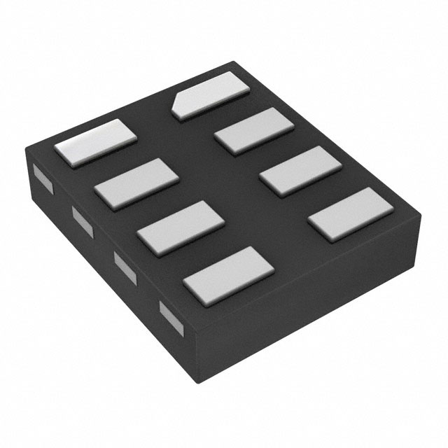
Lihat spesifikasi untuk detail produk.

74LVC2G00RA3-7
Basic Information Overview
- Category: Integrated Circuit (IC)
- Use: Logic Gate
- Characteristics: Dual 2-Input NAND Gate
- Package: SOT353 (SC-88A)
- Essence: High-speed CMOS technology
- Packaging/Quantity: Tape and Reel, 3000 pieces per reel
Specifications
- Supply Voltage Range: 1.65V to 5.5V
- Input Voltage Range: -0.5V to VCC + 0.5V
- Output Voltage Range: GND to VCC
- Operating Temperature Range: -40°C to +125°C
- Propagation Delay: 4.3 ns (typical) at 3.3V supply voltage
Detailed Pin Configuration
The 74LVC2G00RA3-7 has a total of 6 pins: 1. Pin 1: Input A 2. Pin 2: Input B 3. Pin 3: Ground (GND) 4. Pin 4: Output Y 5. Pin 5: Power Supply (VCC) 6. Pin 6: Not Connected (NC)
Functional Features
- Dual 2-Input NAND gate with Schmitt-trigger inputs
- High-speed operation due to low propagation delay
- Wide operating voltage range for compatibility with various systems
- Low power consumption
- High noise immunity
- Balanced propagation delays between the two gates
Advantages
- Compact package size allows for space-saving designs
- Wide operating voltage range enables versatile applications
- Schmitt-trigger inputs provide hysteresis and improve noise immunity
- High-speed operation enhances overall system performance
- Low power consumption contributes to energy-efficient designs
Disadvantages
- Limited number of gates in a single package
- Not suitable for high-power applications
- Sensitivity to electrostatic discharge (ESD) requires proper handling precautions
Working Principles
The 74LVC2G00RA3-7 is based on high-speed CMOS technology, which combines the advantages of both CMOS and TTL logic families. It operates as a dual 2-input NAND gate with Schmitt-trigger inputs. The Schmitt-trigger feature provides hysteresis, allowing the device to tolerate noisy input signals and improve noise immunity.
Detailed Application Field Plans
The 74LVC2G00RA3-7 can be used in various digital logic applications, including but not limited to: - Microcontrollers and microprocessors - Communication systems - Industrial automation - Consumer electronics - Automotive electronics
Detailed and Complete Alternative Models
- SN74LVC2G00DCUR: Dual 2-Input NAND Gate, SOT353 package
- MC74VHC1G00DTT1G: Single 2-Input NAND Gate, SOT23-5 package
- CD4011BM96: Quad 2-Input NAND Gate, SOIC-14 package
- HCF4011BEY: Quad 2-Input NAND Gate, DIP-14 package
(Note: This list is not exhaustive and other alternative models may exist.)
In conclusion, the 74LVC2G00RA3-7 is a dual 2-input NAND gate IC that offers high-speed operation, low power consumption, and wide operating voltage range. Its compact package and Schmitt-trigger inputs make it suitable for various digital logic applications. However, it has limitations in terms of gate count and power handling capabilities. Proper handling and ESD precautions are necessary during usage.
Sebutkan 10 pertanyaan dan jawaban umum terkait penerapan 74LVC2G00RA3-7 dalam solusi teknis
Sure! Here are 10 common questions and answers related to the application of 74LVC2G00RA3-7 in technical solutions:
Q: What is the 74LVC2G00RA3-7? A: The 74LVC2G00RA3-7 is a dual 2-input NAND gate integrated circuit (IC) that operates at low voltage levels.
Q: What is the operating voltage range of the 74LVC2G00RA3-7? A: The operating voltage range of the 74LVC2G00RA3-7 is typically between 1.65V and 5.5V.
Q: What is the maximum output current of the 74LVC2G00RA3-7? A: The maximum output current of the 74LVC2G00RA3-7 is typically around 32mA.
Q: Can the 74LVC2G00RA3-7 be used in battery-powered applications? A: Yes, the 74LVC2G00RA3-7 can be used in battery-powered applications due to its low voltage operation.
Q: What is the propagation delay of the 74LVC2G00RA3-7? A: The propagation delay of the 74LVC2G00RA3-7 is typically around 4.3ns.
Q: Can the 74LVC2G00RA3-7 be used in high-speed applications? A: Yes, the 74LVC2G00RA3-7 can be used in high-speed applications due to its fast switching characteristics.
Q: Is the 74LVC2G00RA3-7 compatible with other logic families? A: Yes, the 74LVC2G00RA3-7 is compatible with a wide range of logic families, including TTL and CMOS.
Q: What is the power supply current consumption of the 74LVC2G00RA3-7? A: The power supply current consumption of the 74LVC2G00RA3-7 is typically around 1.5mA.
Q: Can the 74LVC2G00RA3-7 be used in temperature-sensitive applications? A: Yes, the 74LVC2G00RA3-7 has a wide operating temperature range of -40°C to +125°C, making it suitable for temperature-sensitive applications.
Q: How can I ensure proper signal integrity when using the 74LVC2G00RA3-7? A: To ensure proper signal integrity, it is recommended to follow good PCB layout practices, minimize trace lengths, and use appropriate decoupling capacitors near the IC's power supply pins.
Please note that the answers provided here are general and may vary depending on specific application requirements and datasheet specifications.

