

Lihat spesifikasi untuk detail produk.
Encyclopedia Entry: 74AUP1G08FZ4-7
Product Overview
Category
The 74AUP1G08FZ4-7 belongs to the category of integrated circuits (ICs).
Use
This IC is commonly used as a logic gate, specifically a 2-input AND gate.
Characteristics
- Low power consumption
- High-speed operation
- Wide operating voltage range
- Small package size
- RoHS compliant
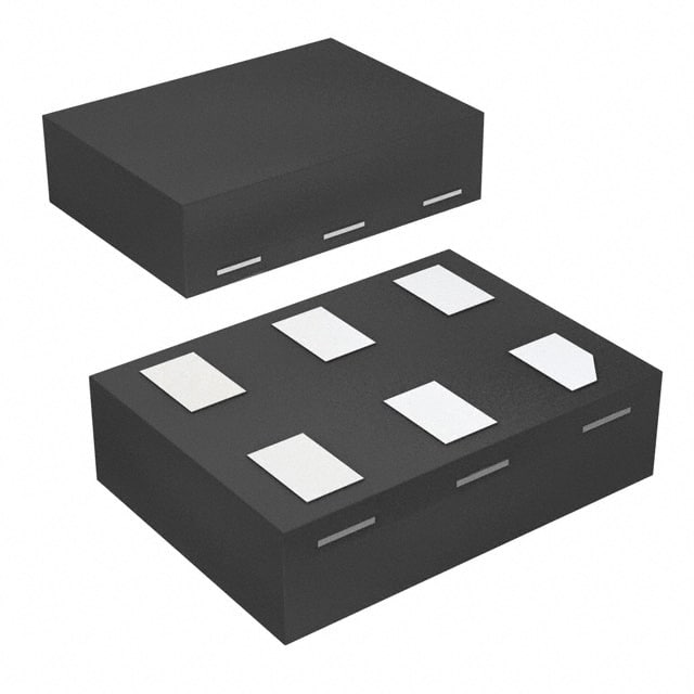
Package and Quantity
The 74AUP1G08FZ4-7 is available in a small form factor package, such as SOT353 or XSON6. It is typically sold in reels or tubes containing multiple units.
Essence
The essence of the 74AUP1G08FZ4-7 lies in its ability to perform logical AND operations with two input signals.
Specifications
- Supply Voltage Range: 0.8V to 3.6V
- Input Voltage Range: 0V to VCC
- Output Voltage Range: 0V to VCC
- Operating Temperature Range: -40°C to +85°C
- Propagation Delay: <5ns
- Maximum Quiescent Current: 10μA
Pin Configuration
The 74AUP1G08FZ4-7 has a simple pin configuration with the following pins: - Pin 1: Input A - Pin 2: Input B - Pin 3: Ground (GND) - Pin 4: Output Y - Pin 5: Power Supply (VCC)
Functional Features
The key functional features of the 74AUP1G08FZ4-7 include: - Logic AND operation: The IC performs a logical AND operation on the input signals A and B, producing the output signal Y. - High-speed operation: The IC operates at a high speed, making it suitable for applications requiring quick response times. - Low power consumption: The IC consumes minimal power, making it ideal for battery-powered devices. - Wide operating voltage range: The IC can operate within a wide voltage range, providing flexibility in various applications.
Advantages and Disadvantages
Advantages
- Small package size allows for space-efficient designs.
- Low power consumption extends battery life in portable devices.
- High-speed operation enables rapid signal processing.
- Wide operating voltage range provides versatility in different voltage environments.
Disadvantages
- Limited to 2-input AND gate functionality, limiting its application scope.
- May not be suitable for complex logic operations requiring multiple inputs.
Working Principles
The 74AUP1G08FZ4-7 works based on the principles of digital logic. It utilizes MOSFET transistors to implement the logical AND operation. When both input signals A and B are high (logic level 1), the output Y is driven high. Otherwise, the output remains low (logic level 0).
Application Field Plans
The 74AUP1G08FZ4-7 finds applications in various fields, including: 1. Consumer electronics: Used in smartphones, tablets, and wearable devices for logic operations. 2. Automotive industry: Employed in vehicle control systems for signal processing and decision-making. 3. Industrial automation: Integrated into control circuits for logical operations in machinery and equipment. 4. Internet of Things (IoT): Utilized in IoT devices for data processing and decision-making.
Alternative Models
Several alternative models with similar functionality to the 74AUP1G08FZ4-7 include: - SN74LVC1G08DBVR - MC74VHC1G08DTT1G - TC7SZ08FU
These alternatives can be considered based on specific requirements and availability.
In conclusion, the 74AUP1G08FZ4-7 is a small-sized, low-power logic gate IC that performs the AND operation. Its high-speed operation, wide voltage range, and compact package make it suitable for various applications in consumer electronics, automotive, industrial automation, and IoT devices. However, its limited functionality as a 2-input AND gate may restrict its use in complex logic operations.
Sebutkan 10 pertanyaan dan jawaban umum terkait penerapan 74AUP1G08FZ4-7 dalam solusi teknis
Sure! Here are 10 common questions and answers related to the application of the 74AUP1G08FZ4-7 in technical solutions:
Q1: What is the 74AUP1G08FZ4-7? A1: The 74AUP1G08FZ4-7 is a single 2-input AND gate IC (integrated circuit) that operates at a voltage level of 0.8V to 3.6V.
Q2: What is the purpose of the 74AUP1G08FZ4-7? A2: The purpose of this IC is to perform logical AND operations on two input signals, producing an output signal based on their logical states.
Q3: What are the key features of the 74AUP1G08FZ4-7? A3: Some key features include low power consumption, wide operating voltage range, high-speed operation, and compatibility with various logic families.
Q4: What are the typical applications of the 74AUP1G08FZ4-7? A4: This IC can be used in various applications such as battery-powered devices, mobile phones, tablets, digital cameras, and other portable electronic devices.
Q5: What is the maximum operating frequency of the 74AUP1G08FZ4-7? A5: The maximum operating frequency of this IC is typically around 500 MHz.
Q6: Can the 74AUP1G08FZ4-7 be used in both CMOS and TTL logic systems? A6: Yes, this IC is compatible with both CMOS and TTL logic systems, making it versatile for different applications.
Q7: What is the power supply voltage range for the 74AUP1G08FZ4-7? A7: The power supply voltage range for this IC is from 0.8V to 3.6V.
Q8: What is the output drive capability of the 74AUP1G08FZ4-7? A8: The output drive capability is typically around 32 mA, allowing it to drive various loads.
Q9: Does the 74AUP1G08FZ4-7 have any built-in protection features? A9: Yes, this IC has built-in ESD (electrostatic discharge) protection, which helps protect it from damage during handling and operation.
Q10: Can the 74AUP1G08FZ4-7 be used in automotive applications? A10: Yes, this IC is suitable for automotive applications as it meets the necessary requirements for automotive electronics.
Please note that these answers are general and may vary depending on specific datasheet specifications and application requirements.