

Lihat spesifikasi untuk detail produk.
Encyclopedia Entry: 74AUP1G00SE-7
Product Overview
Category
The 74AUP1G00SE-7 belongs to the category of integrated circuits (ICs).
Use
This IC is commonly used in electronic devices for signal switching and amplification.
Characteristics
- Low power consumption
- High-speed operation
- Wide operating voltage range
- Small package size
Package
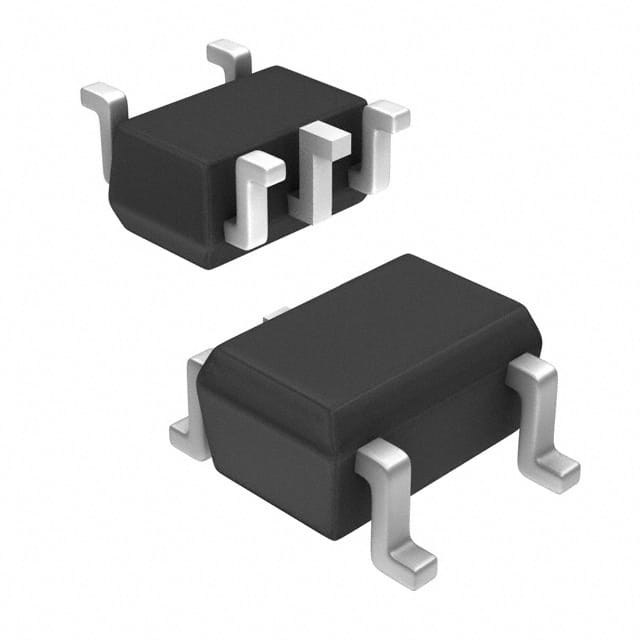
The 74AUP1G00SE-7 is available in a small SOT-353 package.
Essence
The essence of this product lies in its ability to provide reliable and efficient signal switching and amplification in various electronic applications.
Packaging/Quantity
The 74AUP1G00SE-7 is typically packaged in reels, with each reel containing a specific quantity of ICs. The exact quantity may vary depending on the manufacturer's specifications.
Specifications
- Supply Voltage Range: 0.8V to 3.6V
- Input Voltage Range: -0.5V to VCC + 0.5V
- Output Voltage Range: -0.5V to VCC + 0.5V
- Operating Temperature Range: -40°C to +85°C
- Maximum Power Dissipation: 150mW
Detailed Pin Configuration
The 74AUP1G00SE-7 has the following pin configuration:
```
| | --| |-- |____| ```
Pin 1: Input A
Pin 2: Ground (GND)
Pin 3: Output Y
Pin 4: Power Supply (VCC)
Functional Features
- Single 2-input NAND gate functionality
- High-speed operation allows for quick signal processing
- Low power consumption makes it suitable for battery-powered devices
- Wide operating voltage range ensures compatibility with various power supply levels
Advantages
- Compact package size saves board space in electronic designs
- Low power consumption extends battery life in portable devices
- High-speed operation enables efficient signal processing
Disadvantages
- Limited number of inputs and outputs restricts its application in complex circuits
- May not be suitable for high-power applications due to limited power dissipation capability
Working Principles
The 74AUP1G00SE-7 operates based on the principles of digital logic. It utilizes a NAND gate configuration to perform logical operations on input signals, producing an output signal based on the specified truth table.
Detailed Application Field Plans
The 74AUP1G00SE-7 finds applications in various electronic devices, including: - Mobile phones - Tablets - Digital cameras - Portable media players - Wearable devices
Detailed and Complete Alternative Models
Some alternative models that offer similar functionality to the 74AUP1G00SE-7 include: - 74AUP1G00SE-2: Similar specifications but with different package options - 74AUP1G00SE-5: Lower operating voltage range but compatible with certain low-power applications - 74AUP1G00SE-10: Higher power dissipation capability for more demanding applications
In conclusion, the 74AUP1G00SE-7 is a versatile integrated circuit that provides efficient signal switching and amplification in various electronic devices. Its compact size, low power consumption, and high-speed operation make it a popular choice among designers. However, its limited inputs and outputs may restrict its use in complex circuits.
Sebutkan 10 pertanyaan dan jawaban umum terkait penerapan 74AUP1G00SE-7 dalam solusi teknis
Sure! Here are 10 common questions and answers related to the application of 74AUP1G00SE-7 in technical solutions:
Q1: What is the 74AUP1G00SE-7? A1: The 74AUP1G00SE-7 is a single 2-input NAND gate with Schmitt-trigger inputs. It is commonly used in digital logic circuits.
Q2: What is the operating voltage range of the 74AUP1G00SE-7? A2: The 74AUP1G00SE-7 operates within a voltage range of 0.8V to 3.6V.
Q3: What is the maximum output current of the 74AUP1G00SE-7? A3: The maximum output current of the 74AUP1G00SE-7 is typically around 32mA.
Q4: Can the 74AUP1G00SE-7 be used in battery-powered applications? A4: Yes, the 74AUP1G00SE-7 can be used in battery-powered applications due to its low power consumption and wide operating voltage range.
Q5: What is the propagation delay of the 74AUP1G00SE-7? A5: The propagation delay of the 74AUP1G00SE-7 is typically around 2.5ns.
Q6: Can the 74AUP1G00SE-7 be used in high-speed applications? A6: Yes, the 74AUP1G00SE-7 can be used in high-speed applications due to its fast switching speed and low propagation delay.
Q7: Is the 74AUP1G00SE-7 compatible with other logic families? A7: Yes, the 74AUP1G00SE-7 is compatible with a wide range of logic families, including CMOS and TTL.
Q8: Can the 74AUP1G00SE-7 be used in both input and output applications? A8: Yes, the 74AUP1G00SE-7 can be used as both an input and output device in digital logic circuits.
Q9: What is the package type of the 74AUP1G00SE-7? A9: The 74AUP1G00SE-7 is available in various package types, such as SOT353 and XSON6.
Q10: Are there any recommended application circuits for the 74AUP1G00SE-7? A10: Yes, the datasheet of the 74AUP1G00SE-7 provides several recommended application circuits that can be used as a reference for different technical solutions.
Please note that these answers are general and may vary depending on specific design requirements. It is always recommended to refer to the datasheet and consult with technical experts for accurate information.