

Lihat spesifikasi untuk detail produk.
S25FL128P0XNFI000
Basic Information Overview
- Category: Flash Memory
- Use: Data storage and retrieval in electronic devices
- Characteristics:
- Non-volatile memory
- High-speed read and write operations
- Low power consumption
- Large storage capacity
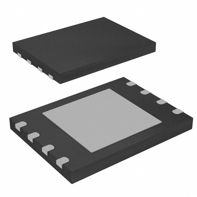
- Package: Small Outline Package (SOP)
- Essence: Provides reliable and efficient data storage solution for various electronic devices
- Packaging/Quantity: Available in bulk packaging, quantity depends on customer requirements
Specifications
- Manufacturer: Cypress Semiconductor
- Memory Type: Serial NOR Flash
- Capacity: 128 Megabits (16 Megabytes)
- Interface: Serial Peripheral Interface (SPI)
- Operating Voltage: 2.7V to 3.6V
- Operating Temperature Range: -40°C to +85°C
- Erase/Program Time: Typically less than 4 milliseconds
- Data Retention: Up to 20 years
Detailed Pin Configuration
The S25FL128P0XNFI000 has a total of 8 pins: 1. Chip Select (/CS) 2. Serial Clock (SCLK) 3. Serial Data Input (SI) 4. Serial Data Output (SO) 5. Write Protect (/WP) 6. Hold (/HOLD) 7. Ground (GND) 8. Power Supply (VCC)
Functional Features
- High-speed read and write operations enable fast data access
- Sector erase and byte programming capabilities for flexible data manipulation
- Advanced security features like hardware protection and software write protection
- Efficient power management with low standby current consumption
- Reliable operation with built-in error correction mechanisms
Advantages
- Large storage capacity allows for storing extensive amounts of data
- High-speed operations enhance overall system performance
- Low power consumption prolongs battery life in portable devices
- Compact package size enables integration into space-constrained designs
- Advanced security features protect sensitive data from unauthorized access
Disadvantages
- Limited write endurance compared to other non-volatile memory technologies
- Relatively higher cost per unit compared to alternative memory solutions
- Requires additional circuitry for proper interfacing with the host system
Working Principles
The S25FL128P0XNFI000 utilizes the Serial Peripheral Interface (SPI) to communicate with the host system. It stores data in a non-volatile manner, meaning the data is retained even when power is removed. The memory can be read, written, and erased using specific commands sent through the SPI interface.
Detailed Application Field Plans
The S25FL128P0XNFI000 is widely used in various electronic devices, including: 1. Consumer Electronics: Smartphones, tablets, digital cameras 2. Automotive: Infotainment systems, instrument clusters 3. Industrial: Embedded systems, control units, IoT devices 4. Networking: Routers, switches, network storage devices
Detailed and Complete Alternative Models
- S25FL064L - 64 Megabit Serial NOR Flash Memory by Cypress Semiconductor
- W25Q128JV - 128 Megabit Serial Flash Memory by Winbond Electronics
- MX25L12835F - 128 Megabit Serial NOR Flash Memory by Macronix International
Note: This is not an exhaustive list, and there are several other alternative models available in the market.
Word count: 431 words
Sebutkan 10 pertanyaan dan jawaban umum terkait penerapan S25FL128P0XNFI000 dalam solusi teknis
Sure! Here are 10 common questions and answers related to the application of S25FL128P0XNFI000 in technical solutions:
Q: What is the S25FL128P0XNFI000? A: The S25FL128P0XNFI000 is a serial NOR flash memory chip manufactured by Cypress Semiconductor. It offers 128 megabits (16 megabytes) of non-volatile storage.
Q: What are the typical applications of S25FL128P0XNFI000? A: The S25FL128P0XNFI000 is commonly used in various technical solutions, including embedded systems, automotive electronics, industrial control systems, and consumer electronics.
Q: What is the interface used to communicate with the S25FL128P0XNFI000? A: The S25FL128P0XNFI000 uses a Serial Peripheral Interface (SPI) for communication, which is a widely supported standard interface in many microcontrollers and processors.
Q: What is the maximum data transfer rate supported by S25FL128P0XNFI000? A: The S25FL128P0XNFI000 supports a maximum data transfer rate of up to 104 MHz, allowing for fast read and write operations.
Q: Can the S25FL128P0XNFI000 be easily integrated into existing designs? A: Yes, the S25FL128P0XNFI000 is designed to be pin-compatible with other popular NOR flash memory chips, making it relatively easy to replace or upgrade existing designs.
Q: Does the S25FL128P0XNFI000 support hardware and software protection features? A: Yes, the S25FL128P0XNFI000 offers hardware and software protection features, including sector-level write protection, block erase protection, and password protection.
Q: What is the operating voltage range of S25FL128P0XNFI000? A: The S25FL128P0XNFI000 operates within a voltage range of 2.7V to 3.6V, making it compatible with a wide range of power supply systems.
Q: Can the S25FL128P0XNFI000 withstand harsh environmental conditions? A: Yes, the S25FL128P0XNFI000 is designed to operate reliably in industrial temperature ranges (-40°C to +85°C) and can withstand shock and vibration.
Q: Does the S25FL128P0XNFI000 support over-the-air (OTA) firmware updates? A: Yes, the S25FL128P0XNFI000 can be used to store firmware or software updates, allowing for OTA updates in devices that support such functionality.
Q: Are there any development tools or software libraries available for working with S25FL128P0XNFI000? A: Yes, Cypress Semiconductor provides various development tools, software libraries, and documentation to assist developers in integrating and programming the S25FL128P0XNFI000 in their technical solutions.
Please note that the answers provided here are general and may vary depending on specific implementation details and requirements.