

Lihat spesifikasi untuk detail produk.
CY7C1041G-10ZSXI
Product Overview
Category
The CY7C1041G-10ZSXI belongs to the category of synchronous static random access memory (SRAM) chips.
Use
This product is commonly used in various electronic devices and systems that require high-speed and reliable data storage and retrieval.
Characteristics
- High-speed operation: The CY7C1041G-10ZSXI offers fast access times, making it suitable for applications that demand quick data processing.
- Low power consumption: This SRAM chip is designed to minimize power consumption, making it energy-efficient.
- High density: With a capacity of 4 megabits (4Mbit), this chip can store a large amount of data.
- Small form factor: The CY7C1041G-10ZSXI comes in a compact package, allowing for space-saving integration into electronic devices.
- Wide temperature range: It operates reliably across a wide temperature range, making it suitable for various environments.
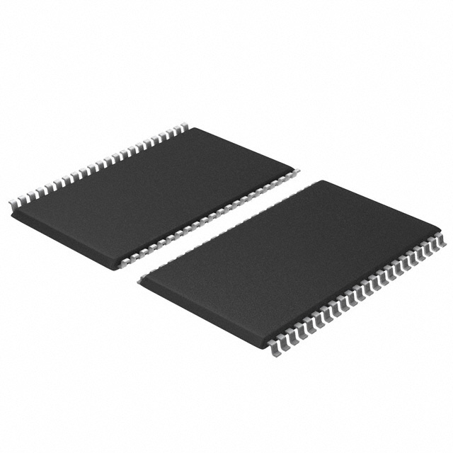
Package and Quantity
The CY7C1041G-10ZSXI is available in a small outline integrated circuit (SOIC) package. It is typically sold in reels containing a specific quantity, such as 250 or 1000 units per reel.
Specifications
- Memory Type: Synchronous SRAM
- Organization: 4M x 1 bit
- Access Time: 10 nanoseconds (ns)
- Voltage Supply: 3.3 volts (V)
- Operating Temperature Range: -40°C to +85°C
- Package Type: SOIC
- Pin Count: 32 pins
Detailed Pin Configuration
The CY7C1041G-10ZSXI has a total of 32 pins, each serving a specific function. Here is a detailed pin configuration:
- VDDQ: Power supply for I/O circuitry
- DQ0-DQ3: Data input/output pins
- VSSQ: Ground for I/O circuitry
- DQ4-DQ7: Data input/output pins
- VDD: Power supply for internal circuitry
- A0-A19: Address input pins
- VSS: Ground for internal circuitry
- CE1, CE2: Chip enable inputs
- WE: Write enable input
- OE: Output enable input
- UB/LB: Upper byte/lower byte control input
- CLK: Clock input
- NC: No connection (reserved)
- NC: No connection (reserved)
- NC: No connection (reserved)
- NC: No connection (reserved)
- NC: No connection (reserved)
- NC: No connection (reserved)
- NC: No connection (reserved)
- NC: No connection (reserved)
- NC: No connection (reserved)
- NC: No connection (reserved)
- NC: No connection (reserved)
- NC: No connection (reserved)
- NC: No connection (reserved)
- NC: No connection (reserved)
- NC: No connection (reserved)
- NC: No connection (reserved)
- NC: No connection (reserved)
- NC: No connection (reserved)
- NC: No connection (reserved)
- VDDQ: Power supply for I/O circuitry
Functional Features
The CY7C1041G-10ZSXI offers the following functional features:
- Synchronous operation: The chip synchronizes its data transfer with an external clock signal, ensuring reliable and accurate data processing.
- Byte control: The upper byte/lower byte control input allows for efficient data manipulation in byte-wide operations.
- Chip enable and write enable inputs: These inputs control the activation of the chip and enable/disable write operations, respectively.
- Output enable input: This input controls the output buffer, allowing for efficient data retrieval.
Advantages and Disadvantages
Advantages
- High-speed operation enables quick data access and processing.
- Low power consumption contributes to energy efficiency.
- Compact form factor allows for space-saving integration.
- Wide temperature range ensures reliable performance in various environments.
Disadvantages
- Limited storage capacity compared to higher-density memory chips.
- Requires an external clock signal for synchronous operation.
Working Principles
The CY7C1041G-10ZSXI operates based on the principles of synchronous static random access memory. It stores and retrieves data using a clock signal to synchronize its internal operations. When the chip is enabled, it reads or writes data from/to the specified memory location based on the address provided. The data is stored in flip-flops within the chip, ensuring fast and reliable access.
Detailed Application Field Plans
The CY7C1041G-10ZSXI finds applications in various electronic devices and systems
Sebutkan 10 pertanyaan dan jawaban umum terkait penerapan CY7C1041G-10ZSXI dalam solusi teknis
Sure! Here are 10 common questions and answers related to the application of CY7C1041G-10ZSXI in technical solutions:
Q1: What is the CY7C1041G-10ZSXI? A1: The CY7C1041G-10ZSXI is a high-speed, low-power, 4-megabit (256K x 16) CMOS static RAM (SRAM) device.
Q2: What are the key features of CY7C1041G-10ZSXI? A2: Some key features include a fast access time of 10 ns, low power consumption, wide voltage range (2.0V to 3.6V), and a small form factor package.
Q3: What are some typical applications of CY7C1041G-10ZSXI? A3: CY7C1041G-10ZSXI can be used in various applications such as networking equipment, telecommunications, industrial automation, medical devices, and automotive systems.
Q4: What is the operating voltage range for CY7C1041G-10ZSXI? A4: The operating voltage range for CY7C1041G-10ZSXI is from 2.0V to 3.6V.
Q5: What is the maximum operating frequency of CY7C1041G-10ZSXI? A5: The maximum operating frequency of CY7C1041G-10ZSXI is 100 MHz.
Q6: Does CY7C1041G-10ZSXI support multiple read and write operations simultaneously? A6: Yes, CY7C1041G-10ZSXI supports multiple read and write operations simultaneously.
Q7: Can CY7C1041G-10ZSXI operate in harsh environments? A7: Yes, CY7C1041G-10ZSXI is designed to operate in a wide temperature range and can withstand harsh environmental conditions.
Q8: What is the power consumption of CY7C1041G-10ZSXI? A8: The power consumption of CY7C1041G-10ZSXI is low, making it suitable for battery-powered devices.
Q9: Does CY7C1041G-10ZSXI have any built-in error correction capabilities? A9: No, CY7C1041G-10ZSXI does not have built-in error correction capabilities. Additional error correction mechanisms may be required if needed.
Q10: Is CY7C1041G-10ZSXI available in different package options? A10: Yes, CY7C1041G-10ZSXI is available in various package options, including SOIC, TSOP, and BGA packages.
Please note that these answers are general and may vary depending on the specific requirements and use cases. It's always recommended to refer to the datasheet or consult with the manufacturer for detailed information.