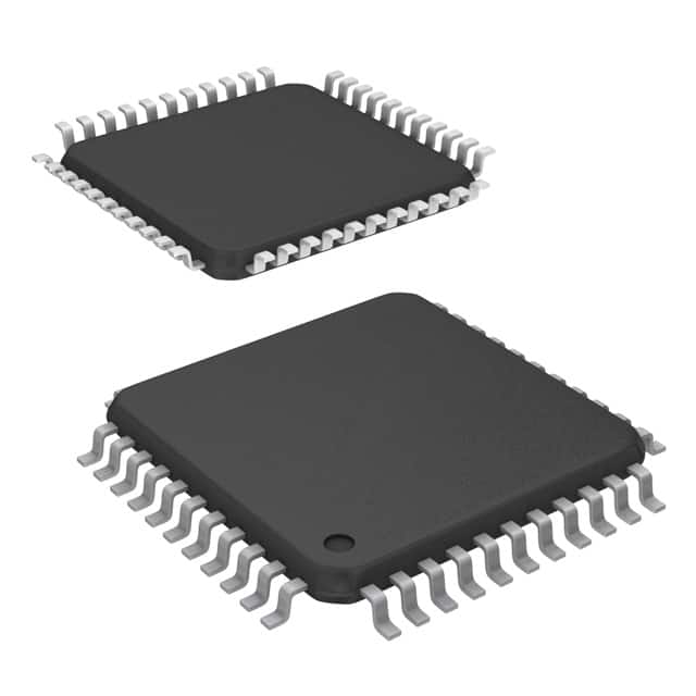
Lihat spesifikasi untuk detail produk.

CY7B9940V-2AXCT
Product Overview
Category
CY7B9940V-2AXCT belongs to the category of integrated circuits (ICs).
Use
This product is commonly used in electronic devices for signal conditioning and clock distribution applications.
Characteristics
- Signal conditioning capabilities
- Clock distribution functionality
- High-speed operation
- Low power consumption
Package
CY7B9940V-2AXCT is available in a small outline integrated circuit (SOIC) package.
Essence
The essence of this product lies in its ability to condition signals and distribute clocks efficiently, making it suitable for various electronic applications.
Packaging/Quantity
CY7B9940V-2AXCT is typically packaged in reels or tubes, with a quantity of 250 units per reel/tube.
Specifications
- Supply voltage: 3.3V
- Operating temperature range: -40°C to +85°C
- Input/output logic levels: CMOS/TTL compatible
- Maximum clock frequency: 200 MHz
- Number of pins: 20
Detailed Pin Configuration
- VDD
- GND
- CLKIN
- CLKOUT0
- CLKOUT1
- CLKOUT2
- CLKOUT3
- CLKOUT4
- CLKOUT5
- CLKOUT6
- CLKOUT7
- CLKOUT8
- CLKOUT9
- CLKOUT10
- CLKOUT11
- CLKOUT12
- CLKOUT13
- CLKOUT14
- CLKOUT15
- NC
Functional Features
- Signal conditioning: CY7B9940V-2AXCT can amplify, filter, or shape input signals to ensure optimal performance.
- Clock distribution: It can distribute a single clock signal to multiple output channels with minimal skew and delay.
Advantages
- High-speed operation: The CY7B9940V-2AXCT can handle clock frequencies up to 200 MHz, making it suitable for demanding applications.
- Low power consumption: This IC is designed to minimize power consumption, contributing to energy-efficient electronic devices.
Disadvantages
- Limited pin count: With only 20 pins, the CY7B9940V-2AXCT may have limitations in complex systems requiring more I/O connections.
Working Principles
CY7B9940V-2AXCT operates by receiving an input clock signal (CLKIN) and conditioning it using internal circuitry. The conditioned clock signals are then distributed to the corresponding output channels (CLKOUT0-CLKOUT15).
Detailed Application Field Plans
The CY7B9940V-2AXCT finds applications in various fields, including:
- Telecommunications: Used in network switches, routers, and communication equipment for clock distribution and signal conditioning.
- Data centers: Employed in servers and storage systems to ensure synchronized clock signals across multiple components.
- Consumer electronics: Integrated into audio/video equipment, gaming consoles, and set-top boxes for signal processing and clock synchronization.
Detailed and Complete Alternative Models
- CY7B9940V-2AXC: Similar to CY7B9940V-2AXCT but without the SOIC package.
- CY7B9940V-2AI: Offers additional features such as programmable delays and frequency multiplication.
- CY7B9940V-2AJ: Provides enhanced EMI/EMC performance for applications with stringent electromagnetic compatibility requirements.
(Note: The above alternative models are provided for reference and may have different specifications and pin configurations.)
In conclusion, the CY7B9940V-2AXCT is a versatile integrated circuit that combines signal conditioning and clock distribution capabilities. Its high-speed operation, low power consumption, and compact package make it suitable for various electronic applications in telecommunications, data centers, and consumer electronics.
Word count: 430 words
Sebutkan 10 pertanyaan dan jawaban umum terkait penerapan CY7B9940V-2AXCT dalam solusi teknis
Sure! Here are 10 common questions and answers related to the application of CY7B9940V-2AXCT in technical solutions:
Question: What is the CY7B9940V-2AXCT?
Answer: The CY7B9940V-2AXCT is a specific model of a programmable skew clock buffer designed for use in high-performance systems.Question: What are the key features of the CY7B9940V-2AXCT?
Answer: Some key features include low output-to-output skew, wide operating frequency range, programmable delay control, and compatibility with various input/output standards.Question: In what applications can the CY7B9940V-2AXCT be used?
Answer: It can be used in applications such as data centers, telecommunications, networking equipment, and other high-speed digital systems that require precise clock distribution.Question: How does the programmable delay control work in the CY7B9940V-2AXCT?
Answer: The programmable delay control allows users to adjust the output skew by programming specific delay values, enabling fine-tuning of clock signals in the system.Question: What is the operating frequency range of the CY7B9940V-2AXCT?
Answer: The operating frequency range is typically from a few megahertz (MHz) up to several gigahertz (GHz), depending on the specific configuration and system requirements.Question: Can the CY7B9940V-2AXCT support multiple input/output standards?
Answer: Yes, it is designed to support various input/output standards such as LVCMOS, LVTTL, HCSL, and LVDS, making it versatile for different system designs.Question: Are there any specific power supply requirements for the CY7B9940V-2AXCT?
Answer: Yes, it typically requires a single power supply voltage in the range of 3.3V to 5V, depending on the specific operating conditions and system specifications.Question: How can I program the delay values in the CY7B9940V-2AXCT?
Answer: The delay values can be programmed through dedicated control pins or via an external serial interface, depending on the specific configuration and system setup.Question: Can the CY7B9940V-2AXCT be used in high-speed data transmission applications?
Answer: Yes, it is suitable for high-speed data transmission applications where precise clock distribution and skew control are critical for maintaining signal integrity.Question: Are there any evaluation boards or reference designs available for the CY7B9940V-2AXCT?
Answer: Yes, Cypress Semiconductor provides evaluation boards and reference designs that can help users understand and test the performance of the CY7B9940V-2AXCT in their specific applications.
Please note that the answers provided here are general and may vary based on specific application requirements and manufacturer documentation.

