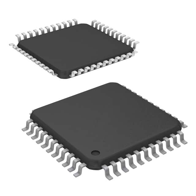
Lihat spesifikasi untuk detail produk.

CY7B9940V-2AXC
Product Overview
Category
CY7B9940V-2AXC belongs to the category of integrated circuits (ICs).
Use
This IC is commonly used in electronic devices for signal conditioning and clock distribution applications.
Characteristics
- Signal Conditioning: The CY7B9940V-2AXC is designed to condition and distribute clock signals effectively.
- Clock Distribution: It provides multiple outputs for distributing clock signals to various components within a system.
Package
The CY7B9940V-2AXC is available in a small outline integrated circuit (SOIC) package.
Essence
The essence of this product lies in its ability to accurately condition and distribute clock signals, ensuring synchronization and proper functioning of electronic devices.
Packaging/Quantity
The CY7B9940V-2AXC is typically packaged in reels or tubes, with a quantity of 250 units per reel/tube.
Specifications
- Supply Voltage: 3.3V
- Operating Temperature Range: -40°C to +85°C
- Output Frequency Range: Up to 200 MHz
- Number of Outputs: 10
- Input Type: LVCMOS/LVTTL
Detailed Pin Configuration
The CY7B9940V-2AXC has a total of 20 pins. The pin configuration is as follows:
- VDD
- GND
- OUT0
- OUT1
- OUT2
- OUT3
- OUT4
- OUT5
- OUT6
- OUT7
- OUT8
- OUT9
- OE#
- CLKIN
- SEL0
- SEL1
- SEL2
- SEL3
- SEL4
- NC
Functional Features
- Clock Conditioning: The CY7B9940V-2AXC conditions the input clock signal to ensure proper voltage levels and signal integrity.
- Clock Distribution: It provides 10 outputs, allowing the distribution of the conditioned clock signal to multiple components within a system.
- Output Enable Control: The OE# pin enables or disables the output signals, providing flexibility in system operation.
Advantages and Disadvantages
Advantages
- Accurate Signal Conditioning: The CY7B9940V-2AXC ensures precise conditioning of clock signals, minimizing signal degradation.
- Multiple Outputs: With 10 outputs, it allows for efficient distribution of clock signals to various components.
- Flexibility: The output enable control feature offers flexibility in enabling or disabling the output signals as required.
Disadvantages
- Limited Frequency Range: The maximum output frequency range of 200 MHz may not be suitable for high-frequency applications.
- Single Input: The CY7B9940V-2AXC has a single input, limiting its use in systems requiring multiple input sources.
Working Principles
The CY7B9940V-2AXC operates by receiving an input clock signal through the CLKIN pin. This signal is then conditioned to meet the desired voltage levels and signal integrity requirements. The conditioned clock signal is distributed to the 10 output pins, allowing synchronization of various components within a system. The output enable control feature enables or disables the output signals based on the state of the OE# pin.
Detailed Application Field Plans
The CY7B9940V-2AXC finds application in various electronic devices and systems that require accurate clock signal conditioning and distribution. Some potential application fields include:
- Communication Systems: Used in networking equipment, routers, and switches to synchronize data transmission.
- Consumer Electronics: Integrated into televisions, audio systems, and gaming consoles for precise timing and synchronization.
- Industrial Automation: Employed in control systems, PLCs, and robotics to ensure accurate timing and coordination of operations.
- Automotive Electronics: Used in vehicle infotainment systems, navigation devices, and advanced driver assistance systems (ADAS) for synchronized functionality.
Detailed and Complete Alternative Models
- CY7B994V-2AXC: Similar to CY7B9940V-2AXC but with 8 outputs instead of 10.
- CY7B9945V-2AXC: Offers additional features such as frequency multiplication and phase-locked loop (PLL) functionality.
- CY7B9942V-2AXC: Provides enhanced input/output voltage compatibility and wider operating temperature range.
These alternative models offer similar functionalities with slight variations to cater to specific application requirements.
Word count: 550 words
Sebutkan 10 pertanyaan dan jawaban umum terkait penerapan CY7B9940V-2AXC dalam solusi teknis
Sure! Here are 10 common questions and answers related to the application of CY7B9940V-2AXC in technical solutions:
Q: What is the CY7B9940V-2AXC? A: The CY7B9940V-2AXC is a high-performance, low-skew, low-jitter clock buffer designed for use in various technical solutions.
Q: What are the key features of the CY7B9940V-2AXC? A: The key features include low output skew, low additive jitter, wide input frequency range, multiple outputs, and compatibility with various voltage levels.
Q: In what applications can I use the CY7B9940V-2AXC? A: The CY7B9940V-2AXC can be used in applications such as networking equipment, telecommunications systems, data centers, and high-speed digital designs.
Q: How many outputs does the CY7B9940V-2AXC have? A: The CY7B9940V-2AXC has a total of 10 outputs, which can be individually controlled and programmed.
Q: What is the input frequency range supported by the CY7B9940V-2AXC? A: The CY7B9940V-2AXC supports an input frequency range from 8 kHz to 350 MHz.
Q: Can I use the CY7B9940V-2AXC with different voltage levels? A: Yes, the CY7B9940V-2AXC is compatible with various voltage levels, including 2.5V, 3.3V, and 5V.
Q: Does the CY7B9940V-2AXC provide any built-in error detection or correction mechanisms? A: No, the CY7B9940V-2AXC does not have built-in error detection or correction mechanisms. It is primarily a clock buffer.
Q: What is the power supply voltage required for the CY7B9940V-2AXC? A: The CY7B9940V-2AXC requires a power supply voltage of 3.3V.
Q: Can I use the CY7B9940V-2AXC in high-speed data transmission applications? A: Yes, the CY7B9940V-2AXC is designed to support high-speed data transmission and can be used in such applications.
Q: Are there any specific layout considerations for using the CY7B9940V-2AXC? A: Yes, it is recommended to follow the layout guidelines provided in the datasheet to ensure optimal performance and minimize signal integrity issues.
Please note that these answers are general and may vary depending on the specific requirements and implementation of your technical solution.

