

Lihat spesifikasi untuk detail produk.
CY7B993V-5AXI
Overview
Product Category
CY7B993V-5AXI belongs to the category of integrated circuits (ICs).
Use
This product is primarily used for clock distribution and fanout applications in electronic devices.
Characteristics
- Clock distribution: CY7B993V-5AXI efficiently distributes clock signals to multiple components within a system.
- Fanout: It provides multiple outputs to drive various devices simultaneously.
- Low jitter: The IC ensures minimal timing errors, resulting in accurate synchronization.
- High-speed operation: It supports high-frequency clock signals for demanding applications.
- Low power consumption: CY7B993V-5AXI is designed to minimize energy consumption.
- Wide operating voltage range: It can operate within a broad voltage range, enhancing compatibility.
Package and Quantity
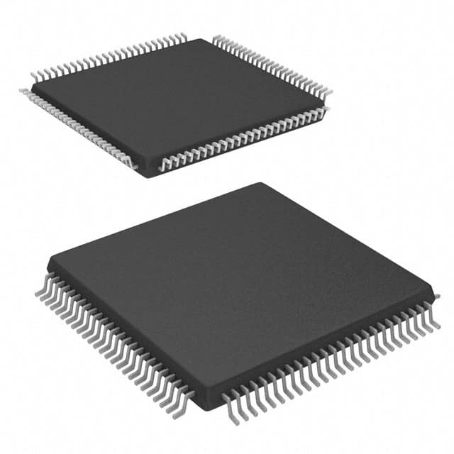
CY7B993V-5AXI is available in a compact package, typically a small outline integrated circuit (SOIC). It is commonly sold in reels or tubes containing a specific quantity, such as 250 or 1000 units per package.
Specifications
- Supply voltage: 3.3V
- Operating temperature range: -40°C to +85°C
- Output frequency range: Up to 200 MHz
- Number of outputs: 10
- Input type: Single-ended or differential
- Output type: LVCMOS
Pin Configuration
The pin configuration of CY7B993V-5AXI is as follows:
- VDD
- GND
- CLKIN
- CLKOUT0
- CLKOUT1
- CLKOUT2
- CLKOUT3
- CLKOUT4
- CLKOUT5
- CLKOUT6
- CLKOUT7
- CLKOUT8
- CLKOUT9
Functional Features
- Clock distribution: CY7B993V-5AXI takes a single input clock signal and distributes it to ten output channels.
- Low jitter: It ensures precise timing synchronization between multiple components.
- Output enable control: Each output channel can be individually enabled or disabled, providing flexibility in system design.
- High-speed operation: The IC supports high-frequency clock signals, making it suitable for demanding applications.
- Easy integration: CY7B993V-5AXI can be easily integrated into existing electronic systems due to its compact size and compatibility with various voltage levels.
Advantages and Disadvantages
Advantages
- Efficient clock distribution to multiple components
- Low jitter for accurate synchronization
- High-speed operation for demanding applications
- Low power consumption
- Wide operating voltage range
Disadvantages
- Limited number of output channels (10)
- Requires external components for proper functionality
Working Principles
CY7B993V-5AXI operates by taking an input clock signal and using internal circuitry to distribute it to the ten output channels. The IC ensures minimal timing errors (jitter) and provides precise synchronization between different components within a system. It achieves this through careful design and optimization of its internal clock distribution network.
Application Field Plans
CY7B993V-5AXI finds applications in various fields, including:
- Telecommunications: Used in networking equipment for clock distribution and synchronization purposes.
- Data centers: Enables precise timing synchronization between servers and networking devices.
- Industrial automation: Provides accurate clock signals for synchronized operation of industrial control systems.
- Consumer electronics: Used in devices requiring multiple synchronized clocks, such as set-top boxes and gaming consoles.
Alternative Models
Other alternative models that offer similar functionality to CY7B993V-5AXI include:
- CY7B9334-100JXC
- SN74LV8154
- CDCLVC1106
These models can be considered as alternatives based on specific requirements and compatibility with the target system.
In conclusion, CY7B993V-5AXI is an integrated circuit primarily used for clock distribution and fanout applications. It offers efficient clock synchronization, low jitter, high-speed operation, and a wide operating voltage range. While it has a limited number of output channels, it provides precise timing synchronization between components within a system. This IC finds applications in telecommunications, data centers, industrial automation, and consumer electronics. Alternative models such as CY7B9334-100JXC, SN74LV8154, and CDCLVC1106 offer similar functionality and can be considered based on specific requirements.
Sebutkan 10 pertanyaan dan jawaban umum terkait penerapan CY7B993V-5AXI dalam solusi teknis
Sure! Here are 10 common questions and answers related to the application of CY7B993V-5AXI in technical solutions:
Q: What is the CY7B993V-5AXI? A: The CY7B993V-5AXI is a high-performance, low-skew, low-jitter clock buffer designed for use in various electronic systems.
Q: What are the key features of the CY7B993V-5AXI? A: The key features include 10 outputs, low output skew, low additive jitter, wide input frequency range, and compatibility with different voltage levels.
Q: In what applications can I use the CY7B993V-5AXI? A: The CY7B993V-5AXI can be used in applications such as data centers, telecommunications, networking equipment, industrial automation, and high-speed digital systems.
Q: How many outputs does the CY7B993V-5AXI have? A: The CY7B993V-5AXI has 10 outputs, which can be used to distribute clock signals to multiple components or subsystems.
Q: What is the output skew of the CY7B993V-5AXI? A: The CY7B993V-5AXI has a low output skew of typically less than 50 ps, ensuring accurate synchronization between different parts of a system.
Q: Can the CY7B993V-5AXI handle different input frequencies? A: Yes, the CY7B993V-5AXI supports a wide input frequency range from 8 kHz to 350 MHz, making it suitable for various clocking requirements.
Q: Is the CY7B993V-5AXI compatible with different voltage levels? A: Yes, the CY7B993V-5AXI is compatible with both 3.3V and 2.5V voltage levels, providing flexibility in system design.
Q: Does the CY7B993V-5AXI have any built-in jitter reduction features? A: Yes, the CY7B993V-5AXI incorporates a low additive jitter PLL (Phase-Locked Loop) to minimize clock signal distortion and improve overall system performance.
Q: Can I use the CY7B993V-5AXI in high-speed data transmission applications? A: Absolutely! The CY7B993V-5AXI is designed to handle high-speed data transmission up to 350 MHz, making it suitable for demanding applications.
Q: Are there any evaluation boards or reference designs available for the CY7B993V-5AXI? A: Yes, Cypress Semiconductor provides evaluation boards and reference designs that can help you quickly prototype and integrate the CY7B993V-5AXI into your system.
Please note that these answers are general and may vary depending on specific application requirements. It's always recommended to refer to the datasheet and consult with technical experts for detailed information.