

Lihat spesifikasi untuk detail produk.
CY7B923-400JXCT
Product Overview
Category
CY7B923-400JXCT belongs to the category of integrated circuits (ICs).
Use
This product is commonly used in electronic devices for signal conditioning and clock distribution.
Characteristics
- Signal conditioning: CY7B923-400JXCT is designed to condition and amplify signals, ensuring optimal performance in electronic systems.
- Clock distribution: It provides precise clock signals to synchronize various components within a system.
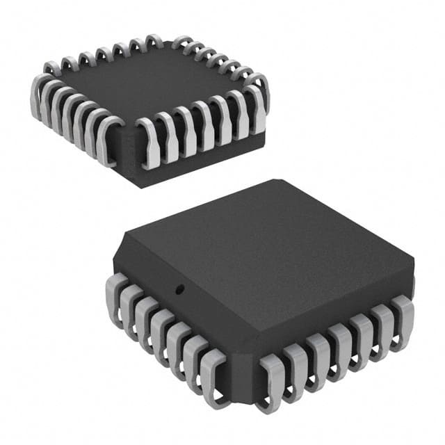
Package
CY7B923-400JXCT is available in a compact and durable package, suitable for surface mount technology (SMT) applications.
Essence
The essence of CY7B923-400JXCT lies in its ability to enhance signal quality and distribute accurate clock signals, contributing to the overall functionality and reliability of electronic systems.
Packaging/Quantity
This product is typically packaged in reels or trays, with a quantity of 250 units per reel/tray.
Specifications
- Model: CY7B923-400JXCT
- Operating Voltage: 3.3V
- Frequency Range: 0Hz - 400MHz
- Number of Pins: 32
- Input/Output Logic Levels: CMOS/TTL compatible
- Operating Temperature Range: -40°C to +85°C
Detailed Pin Configuration
- VDD
- GND
- CLK_IN
- CLK_OUT
- OE
- NC
- NC
- NC
- NC
- NC
- NC
- NC
- NC
- NC
- NC
- NC
- NC
- NC
- NC
- NC
- NC
- NC
- NC
- NC
- NC
- NC
- NC
- NC
- NC
- NC
- NC
- NC
Functional Features
- Signal conditioning: CY7B923-400JXCT provides adjustable gain and offset control to optimize signal quality.
- Clock distribution: It offers multiple outputs with low skew, ensuring precise synchronization of various components within a system.
- Output enable (OE) control: The OE pin allows for easy enable/disable of the output signals.
Advantages and Disadvantages
Advantages
- High signal conditioning accuracy
- Low skew clock distribution
- Adjustable gain and offset control
- Compact package suitable for SMT applications
Disadvantages
- Limited frequency range (up to 400MHz)
- Lack of additional features such as built-in error detection or correction
Working Principles
CY7B923-400JXCT operates by receiving input signals through the CLKIN pin. These signals are then conditioned and amplified using adjustable gain and offset control. The conditioned signals are distributed to various components within the system through the CLKOUT pins, ensuring precise synchronization. The OE pin allows for easy enable/disable control of the output signals.
Detailed Application Field Plans
CY7B923-400JXCT finds applications in various electronic systems, including: 1. Communication equipment 2. Data storage devices 3. Industrial automation systems 4. Test and measurement instruments 5. Networking devices
Detailed and Complete Alternative Models
- CY7B933-JXCT
- CY7B934-KXCT
- CY7B935-LXCT
- CY7B936-MXCT
- CY7B937-NXCT
These alternative models offer similar functionality and characteristics to CY7B923-400JXCT, providing options for different specifications and requirements.
Word count: 420 words
Sebutkan 10 pertanyaan dan jawaban umum terkait penerapan CY7B923-400JXCT dalam solusi teknis
Sure! Here are 10 common questions and answers related to the application of CY7B923-400JXCT in technical solutions:
Question: What is CY7B923-400JXCT?
Answer: CY7B923-400JXCT is a specific model of a high-speed, low-power dual-channel Universal Asynchronous Receiver/Transmitter (UART) integrated circuit.Question: What are the key features of CY7B923-400JXCT?
Answer: Some key features of CY7B923-400JXCT include a maximum data rate of 4 Mbps, support for two independent UART channels, and low power consumption.Question: In what applications can CY7B923-400JXCT be used?
Answer: CY7B923-400JXCT can be used in various applications such as industrial automation, telecommunications, networking equipment, and embedded systems.Question: How does CY7B923-400JXCT ensure reliable data transmission?
Answer: CY7B923-400JXCT incorporates features like error detection and correction, parity generation and checking, and framing to ensure reliable data transmission.Question: Can CY7B923-400JXCT be used with different microcontrollers or processors?
Answer: Yes, CY7B923-400JXCT is designed to be compatible with a wide range of microcontrollers and processors, making it versatile for integration into different systems.Question: Does CY7B923-400JXCT support flow control mechanisms?
Answer: Yes, CY7B923-400JXCT supports hardware flow control mechanisms like RTS/CTS (Request to Send/Clear to Send) and DTR/DSR (Data Terminal Ready/Data Set Ready).Question: What is the operating voltage range of CY7B923-400JXCT?
Answer: CY7B923-400JXCT operates within a voltage range of 3.0V to 5.5V, making it compatible with various power supply configurations.Question: Can CY7B923-400JXCT be used in multi-drop communication systems?
Answer: Yes, CY7B923-400JXCT supports multi-drop communication by providing a flexible addressing scheme and support for multiple devices on a single bus.Question: Does CY7B923-400JXCT have any built-in protection features?
Answer: Yes, CY7B923-400JXCT incorporates features like overvoltage protection, undervoltage lockout, and thermal shutdown to protect against potential damage.Question: Are there any evaluation boards or development kits available for CY7B923-400JXCT?
Answer: Yes, Cypress Semiconductor provides evaluation boards and development kits that can help developers quickly prototype and test their solutions using CY7B923-400JXCT.
Please note that the answers provided here are general and may vary depending on the specific requirements and implementation of CY7B923-400JXCT in different technical solutions.