

Lihat spesifikasi untuk detail produk.
CY62147G18-55BVXI
Product Overview
Category
CY62147G18-55BVXI belongs to the category of semiconductor memory devices.
Use
This product is primarily used for data storage and retrieval in electronic devices such as computers, smartphones, and other digital systems.
Characteristics
- High-speed performance: The CY62147G18-55BVXI offers fast read and write speeds, enabling efficient data processing.
- Low power consumption: This device is designed to operate with minimal power requirements, making it suitable for battery-powered devices.
- Compact package: The CY62147G18-55BVXI is available in a small form factor, allowing for space-efficient integration into various electronic systems.
- High reliability: With advanced error correction techniques and robust design, this product ensures reliable data storage and retrieval.
- Wide temperature range: The CY62147G18-55BVXI can operate reliably across a broad temperature range, making it suitable for various environments.
Package and Quantity
The CY62147G18-55BVXI is typically packaged in a compact integrated circuit (IC) package. It is commonly available in tape and reel packaging, with a quantity of 1000 units per reel.
Specifications
- Memory Type: Static Random Access Memory (SRAM)
- Organization: 1M x 16 bits
- Operating Voltage: 2.5V - 3.6V
- Access Time: 55ns
- Standby Current: 10μA (typical)
- Operating Temperature Range: -40°C to +85°C
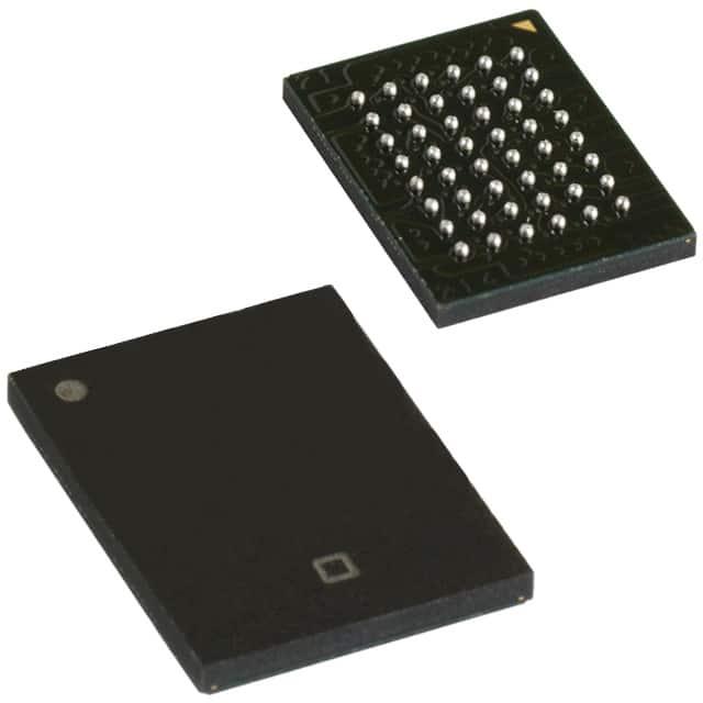
- Package Type: BGA (Ball Grid Array)
Pin Configuration
The CY62147G18-55BVXI features a ball grid array (BGA) package with a total of 48 pins. The pin configuration is as follows:
```
Pin Name Description
1 VCC Power Supply 2 A0-A19 Address Inputs 3 DQ0-DQ15 Data Inputs/Outputs 4 WE# Write Enable 5 OE# Output Enable 6 CE# Chip Enable 7 UB/LB# Upper Byte/Lower Byte Control 8 CLK Clock Input 9-48 NC No Connection ```
Functional Features
- Random Access: The CY62147G18-55BVXI allows for random access to any memory location, enabling efficient data retrieval.
- High-Speed Operation: With a fast access time of 55ns, this device ensures quick data processing.
- Low Power Consumption: The CY62147G18-55BVXI operates with low power requirements, extending the battery life of portable devices.
- Easy Integration: This product is designed for easy integration into various electronic systems, thanks to its compact package and standard interface.
Advantages and Disadvantages
Advantages
- High-speed performance enables efficient data processing.
- Low power consumption prolongs battery life in portable devices.
- Compact package allows for space-efficient integration.
- Wide temperature range ensures reliable operation in various environments.
Disadvantages
- Limited storage capacity compared to other memory technologies.
- Volatile memory requires constant power supply to retain data.
Working Principles
The CY62147G18-55BVXI utilizes static random access memory (SRAM) technology. It stores data in a volatile manner, meaning that it requires a continuous power supply to retain information. The SRAM cells within the device use flip-flops to store each bit of data. When an address is provided, the corresponding data can be read or written to the memory cell.
Application Field Plans
The CY62147G18-55BVXI finds applications in various electronic devices and systems, including: - Computers and laptops - Smartphones and tablets - Networking equipment - Automotive electronics - Industrial control systems
Alternative Models
For users seeking alternative options, the following models offer similar functionality to the CY62147G18-55BVXI: - CY62146EV30-45ZSXI - IS61LV25616AL-10TLI - AS6C4008-55BIN
These alternatives provide comparable specifications and can be considered as substitutes for the CY62147G18-55BVXI in specific applications.
In conclusion, the CY62147G18-55BVXI is a high-performance SRAM device that offers fast operation, low power consumption, and reliable data storage. Its compact package and wide temperature range make it suitable for various electronic systems. However, its limited storage capacity and volatile nature should be considered when selecting this product for specific applications.
Sebutkan 10 pertanyaan dan jawaban umum terkait penerapan CY62147G18-55BVXI dalam solusi teknis
Question: What is the operating voltage range of CY62147G18-55BVXI?
Answer: The operating voltage range of CY62147G18-55BVXI is 2.7V to 3.6V.Question: What is the maximum clock frequency supported by CY62147G18-55BVXI?
Answer: CY62147G18-55BVXI supports a maximum clock frequency of 55 MHz.Question: Can CY62147G18-55BVXI be used in battery-powered devices?
Answer: Yes, CY62147G18-55BVXI can be used in battery-powered devices as it operates within a low voltage range and has low power consumption.Question: What is the capacity of CY62147G18-55BVXI?
Answer: CY62147G18-55BVXI has a capacity of 4 Megabits (4Mbit) or 512 Kilobytes (512KB).Question: Is CY62147G18-55BVXI compatible with other memory devices?
Answer: Yes, CY62147G18-55BVXI is compatible with other memory devices as it follows industry-standard protocols.Question: Can CY62147G18-55BVXI be used in automotive applications?
Answer: Yes, CY62147G18-55BVXI is suitable for automotive applications as it meets the required temperature and reliability standards.Question: Does CY62147G18-55BVXI support multiple read and write operations simultaneously?
Answer: No, CY62147G18-55BVXI does not support simultaneous multiple read and write operations.Question: What is the access time of CY62147G18-55BVXI?
Answer: The access time of CY62147G18-55BVXI is 55 ns.Question: Can CY62147G18-55BVXI be used in industrial control systems?
Answer: Yes, CY62147G18-55BVXI can be used in industrial control systems as it operates within the required voltage and temperature ranges.Question: Does CY62147G18-55BVXI have built-in error correction capabilities?
Answer: No, CY62147G18-55BVXI does not have built-in error correction capabilities.