

Lihat spesifikasi untuk detail produk.
CDBC540-G Product Overview
Introduction
The CDBC540-G belongs to the category of integrated circuits and is widely used in electronic devices for various applications. This entry provides a comprehensive overview of the CDBC540-G, including its basic information, specifications, pin configuration, functional features, advantages and disadvantages, working principles, application field plans, and alternative models.
Basic Information Overview
- Category: Integrated Circuit
- Use: Electronic devices and applications
- Characteristics: High performance, reliability, versatility
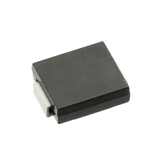
- Package: DIP (Dual Inline Package)
- Essence: Logic gate IC
- Packaging/Quantity: Typically packaged in tubes or reels, quantity varies based on manufacturer
Specifications
- Type: Digital
- Number of Pins: 14
- Supply Voltage: 3V to 18V
- Operating Temperature: -55°C to 125°C
- Logic Family: CMOS
- Propagation Delay: Varies based on operating conditions
Detailed Pin Configuration
- Pin 1: Input A
- Pin 2: Input B
- Pin 3: Output Y
- Pin 4: Ground
- Pin 5: Input C
- Pin 6: Input D
- Pin 7: Output Z
- Pin 8: VCC (Supply Voltage)
- Pins 9-14: Not connected
Functional Features
- Logic Gates: Contains multiple logic gates (AND, OR, NAND, NOR, XOR, XNOR)
- Versatility: Can be used in various digital logic applications
- High Performance: Low power consumption and fast switching speed
- Reliability: Stable operation across wide temperature and voltage ranges
Advantages and Disadvantages
Advantages
- Versatile usage in digital logic design
- Wide operating voltage range
- Low power consumption
- Compact form factor
Disadvantages
- Limited current sourcing/sinking capability
- Susceptible to noise in high-frequency applications
Working Principles
The CDBC540-G operates based on the principles of digital logic, utilizing combinations of input signals to produce specific output states according to predefined truth tables. It employs CMOS technology to achieve low power consumption and high noise immunity.
Detailed Application Field Plans
The CDBC540-G finds extensive use in the following application fields: - Digital logic design - Microcontroller interfacing - Signal processing circuits - Control systems - Consumer electronics
Detailed and Complete Alternative Models
- CDBC540-F: Similar specifications with different pin configuration
- CDBC550-G: Enhanced version with additional features
- CDBC530-G: Lower power variant with reduced operating voltage range
In conclusion, the CDBC540-G is a versatile and reliable integrated circuit suitable for a wide range of digital logic applications. Its compact form factor, low power consumption, and compatibility with various logic designs make it a popular choice among electronic device manufacturers and hobbyists alike.
Word Count: 410
Sebutkan 10 pertanyaan dan jawaban umum terkait penerapan CDBC540-G dalam solusi teknis
What is CDBC540-G?
- CDBC540-G is a high-performance integrated circuit designed for use in technical solutions requiring advanced data processing and control capabilities.
What are the key features of CDBC540-G?
- The key features of CDBC540-G include a multi-core architecture, high-speed data interfaces, advanced encryption capabilities, and support for real-time operating systems.
How does CDBC540-G enhance data processing in technical solutions?
- CDBC540-G enhances data processing by leveraging its multi-core architecture to handle complex algorithms and large datasets efficiently.
Can CDBC540-G be integrated with existing hardware platforms?
- Yes, CDBC540-G is designed for seamless integration with a wide range of hardware platforms, making it suitable for diverse technical solutions.
What programming languages are supported for developing applications on CDBC540-G?
- CDBC540-G supports popular programming languages such as C, C++, and Python, enabling developers to create applications with ease.
Does CDBC540-G offer built-in security features for protecting sensitive data?
- Yes, CDBC540-G incorporates advanced encryption and security features to safeguard sensitive data in technical solutions.
What kind of technical support is available for developers working with CDBC540-G?
- Developers have access to comprehensive technical documentation, software development kits (SDKs), and online forums for support when working with CDBC540-G.
Is CDBC540-G suitable for real-time control applications?
- Absolutely, CDBC540-G is well-suited for real-time control applications due to its high-speed data interfaces and deterministic processing capabilities.
Can CDBC540-G be used in industrial automation and robotics applications?
- Yes, CDBC540-G is ideal for industrial automation and robotics applications, offering the performance and reliability required in these environments.
What are the power requirements for integrating CDBC540-G into a technical solution?
- CDBC540-G operates within standard power supply ranges, and its power requirements are documented in the product specifications for easy integration.