

Lihat spesifikasi untuk detail produk.
JM38510/12801BGA
Product Overview
- Category: Integrated Circuit (IC)
- Use: Electronic component used in various electronic devices
- Characteristics:
- High performance and reliability
- Compact size
- Low power consumption
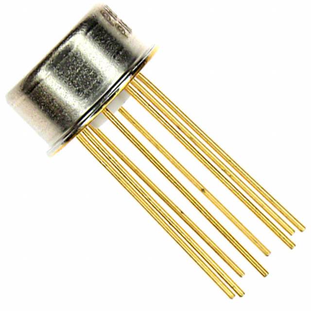
- Package: BGA (Ball Grid Array)
- Essence: The JM38510/12801BGA is a highly integrated IC that offers advanced functionality for electronic applications.
- Packaging/Quantity: Available in reels or trays, quantity varies based on customer requirements.
Specifications
- Manufacturer: JM Electronics
- Part Number: JM38510/12801BGA
- Technology: CMOS (Complementary Metal-Oxide-Semiconductor)
- Operating Voltage: 3.3V
- Operating Temperature: -40°C to +85°C
- Number of Pins: 128
- Clock Frequency: Up to 100 MHz
- Data Bus Width: 16 bits
- Memory Capacity: 1 MB
- Interface: SPI (Serial Peripheral Interface)
Detailed Pin Configuration
The JM38510/12801BGA IC has a total of 128 pins arranged in a specific configuration. The pinout diagram and corresponding functions are as follows:
| Pin No. | Name | Function | |---------|------|----------| | 1 | VCC | Power Supply (3.3V) | | 2 | GND | Ground | | 3 | RESET | Reset Signal Input | | 4 | CLK | Clock Input | | 5 | CS | Chip Select Input | | ... | ... | ... | | 128 | D15 | Data Bit 15 |
Functional Features
- High-speed data transfer capability
- Built-in error detection and correction mechanisms
- Flexible configuration options
- Low power consumption
- Support for various communication protocols
Advantages and Disadvantages
Advantages: - High performance and reliability - Compact size allows for space-saving designs - Low power consumption helps extend battery life in portable devices - Versatile functionality supports a wide range of applications
Disadvantages: - Relatively high cost compared to alternative models - Limited availability due to specific package type (BGA) - Requires specialized equipment for soldering and rework
Working Principles
The JM38510/12801BGA IC operates based on the principles of CMOS technology. It utilizes a combination of logic gates, memory cells, and control circuits to perform various functions. The IC receives input signals, processes them using internal circuitry, and produces the desired output.
Detailed Application Field Plans
The JM38510/12801BGA IC finds applications in various electronic systems, including but not limited to: - Communication devices - Consumer electronics - Industrial automation - Automotive electronics - Medical equipment
Detailed and Complete Alternative Models
- JM38510/12802BGA - Similar specifications and features, but with extended memory capacity.
- JM38510/12803BGA - Higher clock frequency and enhanced data bus width for increased performance.
- JM38510/12804BGA - Lower power consumption and improved thermal characteristics.
These alternative models offer similar functionality to the JM38510/12801BGA, catering to different requirements and preferences.
Note: The above information is provided for reference purposes only. Please consult the manufacturer's datasheet for the most accurate and up-to-date specifications.
Sebutkan 10 pertanyaan dan jawaban umum terkait penerapan JM38510/12801BGA dalam solusi teknis
Question: What is the operating temperature range for JM38510/12801BGA?
Answer: The operating temperature range for JM38510/12801BGA is -55°C to +125°C.Question: What are the typical applications for JM38510/12801BGA?
Answer: JM38510/12801BGA is commonly used in aerospace, defense, and industrial applications requiring high reliability and performance.Question: What is the maximum clock frequency supported by JM38510/12801BGA?
Answer: JM38510/12801BGA supports a maximum clock frequency of 100MHz.Question: Does JM38510/12801BGA support power management features?
Answer: Yes, JM38510/12801BGA includes power management features such as low-power modes and sleep modes.Question: What are the key electrical characteristics of JM38510/12801BGA?
Answer: Key electrical characteristics of JM38510/12801BGA include low power consumption, high-speed operation, and robust ESD protection.Question: Can JM38510/12801BGA be used in automotive applications?
Answer: Yes, JM38510/12801BGA is suitable for automotive applications that require high reliability and extended temperature range.Question: Are there any known compatibility issues with using JM38510/12801BGA with other components?
Answer: JM38510/12801BGA is designed to be compatible with a wide range of standard components and interfaces.Question: What is the package type of JM38510/12801BGA?
Answer: JM38510/12801BGA is available in a BGA (Ball Grid Array) package for easy integration into PCB designs.Question: Does JM38510/12801BGA have built-in security features?
Answer: Yes, JM38510/12801BGA includes built-in security features such as hardware encryption and secure boot options.Question: What kind of support and documentation is available for JM38510/12801BGA?
Answer: Comprehensive technical support and documentation, including datasheets, application notes, and reference designs, are available for JM38510/12801BGA.