

Lihat spesifikasi untuk detail produk.
ADCMP562BRQ
Product Overview
- Category: Analog-to-Digital Converter (ADC)
- Use: Converts analog signals into digital data for processing or storage
- Characteristics: High-speed, low-power, precision conversion
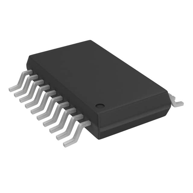
- Package: Small outline integrated circuit (SOIC)
- Essence: Provides accurate and reliable conversion of analog signals
- Packaging/Quantity: Available in reels of 250 units
Specifications
- Resolution: 12 bits
- Conversion Rate: 1 MSPS (Mega Samples Per Second)
- Input Voltage Range: 0V to Vref
- Power Supply: 2.7V to 5.5V
- Operating Temperature Range: -40°C to +85°C
Pin Configuration
The ADCMP562BRQ has the following pin configuration:
- VDD: Power supply voltage
- VREF: Reference voltage input
- VIN: Analog input voltage
- GND: Ground reference
- CLK: Clock input
- CS: Chip select input
- DOUT: Digital output
- DGND: Digital ground reference
Functional Features
- High-speed conversion with a sampling rate of 1 MSPS
- Low power consumption for energy-efficient operation
- Precise and accurate conversion with 12-bit resolution
- Wide input voltage range allows for versatile applications
- Small package size for space-constrained designs
- Easy integration into existing systems with standard interface protocols
Advantages and Disadvantages
Advantages: - High-speed conversion enables real-time data acquisition - Low power consumption prolongs battery life in portable devices - Accurate conversion ensures reliable measurement results - Versatile input voltage range accommodates various signal levels - Compact package size facilitates integration into small form factor designs
Disadvantages: - Limited resolution compared to higher-end ADCs - May require additional external components for specific applications - Operating temperature range may restrict usage in extreme environments
Working Principles
The ADCMP562BRQ utilizes a successive approximation register (SAR) architecture to convert analog signals into digital data. It samples the input voltage at a high rate and compares it to a reference voltage. By iteratively adjusting the digital code, the converter converges to a value that represents the input voltage with the desired resolution.
Detailed Application Field Plans
The ADCMP562BRQ finds application in various fields, including:
- Industrial Automation: Precise measurement of sensor outputs
- Medical Devices: Accurate data acquisition from physiological sensors
- Communications: Signal processing in wireless communication systems
- Test and Measurement: High-speed data acquisition for analysis
- Automotive: Monitoring and control of vehicle parameters
Alternative Models
For alternative options, consider the following ADCs:
- ADCMP563BRQ: 14-bit resolution, higher accuracy
- ADCMP564BRQ: 16-bit resolution, ultra-high precision
- ADCMP565BRQ: 10-bit resolution, lower cost option
These models offer different resolutions and features to suit specific application requirements.
Word count: 314 words
Sebutkan 10 pertanyaan dan jawaban umum terkait penerapan ADCMP562BRQ dalam solusi teknis
Sure! Here are 10 common questions and answers related to the application of ADCMP562BRQ in technical solutions:
Q: What is ADCMP562BRQ? A: ADCMP562BRQ is a high-speed comparator integrated circuit (IC) that can be used in various technical applications.
Q: What is the operating voltage range of ADCMP562BRQ? A: The operating voltage range of ADCMP562BRQ is typically between 2.7V and 5.5V.
Q: What is the maximum input voltage range of ADCMP562BRQ? A: The maximum input voltage range of ADCMP562BRQ is typically between -0.3V and VCC + 0.3V.
Q: What is the output voltage swing of ADCMP562BRQ? A: The output voltage swing of ADCMP562BRQ is typically rail-to-rail, meaning it can swing close to the supply voltage rails.
Q: What is the response time of ADCMP562BRQ? A: The response time of ADCMP562BRQ is typically very fast, with rise and fall times in the nanosecond range.
Q: Can ADCMP562BRQ operate in both single-ended and differential mode? A: Yes, ADCMP562BRQ can operate in both single-ended and differential mode, providing flexibility in different applications.
Q: Is ADCMP562BRQ suitable for low-power applications? A: Yes, ADCMP562BRQ has a low quiescent current and can be used in low-power applications.
Q: Does ADCMP562BRQ have built-in hysteresis? A: Yes, ADCMP562BRQ has built-in hysteresis, which helps to prevent oscillations and improve noise immunity.
Q: Can ADCMP562BRQ tolerate overvoltage conditions? A: ADCMP562BRQ has built-in protection features that allow it to tolerate limited overvoltage conditions.
Q: What are some typical applications of ADCMP562BRQ? A: ADCMP562BRQ can be used in various applications such as level shifting, line receivers, window comparators, and motor control systems.
Please note that the answers provided here are general and may vary depending on specific datasheet specifications and application requirements.