

Lihat spesifikasi untuk detail produk.
AD5314BRM
Product Overview
Category
AD5314BRM belongs to the category of digital-to-analog converters (DACs).
Use
The AD5314BRM is used to convert digital signals into analog voltages. It finds applications in various electronic systems where precise analog voltage outputs are required.
Characteristics
- High resolution: The AD5314BRM provides a resolution of 12 bits, allowing for fine-grained control over the analog output.
- Low power consumption: This DAC operates at low power, making it suitable for battery-powered devices.
- Fast settling time: The AD5314BRM offers fast settling time, ensuring quick and accurate conversion of digital signals to analog voltages.
- Wide operating voltage range: It can operate within a wide voltage range, making it compatible with different power supply configurations.
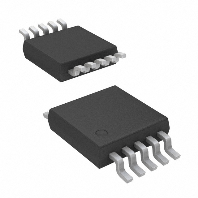
Package
The AD5314BRM comes in a small outline integrated circuit (SOIC) package, which provides ease of integration into various electronic systems.
Essence
The essence of the AD5314BRM lies in its ability to accurately convert digital signals into precise analog voltages, enabling the control of analog circuits and systems.
Packaging/Quantity
The AD5314BRM is typically available in reels containing a quantity of 250 units per reel.
Specifications
- Resolution: 12 bits
- Supply Voltage Range: 2.7V to 5.5V
- Operating Temperature Range: -40°C to +105°C
- Output Voltage Range: 0V to Vref
- Interface: Serial Peripheral Interface (SPI)
- Package Type: SOIC
Detailed Pin Configuration
The AD5314BRM has a total of 16 pins. The pin configuration is as follows:
- VDD: Power supply voltage input
- VREF: Reference voltage input
- AGND: Analog ground
- AOUT0: Analog output channel 0
- AOUT1: Analog output channel 1
- AOUT2: Analog output channel 2
- AOUT3: Analog output channel 3
- DGND: Digital ground
- SDI: Serial data input
- SDO: Serial data output
- SCLK: Serial clock input
- SYNC: Chip select input
- LDAC: Load DAC input
- CLR: Clear input
- REFIN: Reference voltage output
- VLOGIC: Logic supply voltage input
Functional Features
- High-resolution digital-to-analog conversion
- SPI interface for easy integration with microcontrollers and other digital systems
- Low power consumption for energy-efficient operation
- Fast settling time for quick response to digital input changes
- Internal reference voltage for simplified system design
Advantages and Disadvantages
Advantages
- High resolution allows for precise analog voltage control
- Low power consumption makes it suitable for battery-powered devices
- Fast settling time ensures accurate and responsive analog output
- Wide operating voltage range provides flexibility in power supply configurations
Disadvantages
- Limited number of analog output channels (4 channels)
- Requires an external reference voltage for accurate conversion
Working Principles
The AD5314BRM operates by receiving digital input signals through the SPI interface. These digital signals are then converted into corresponding analog voltages using a high-resolution digital-to-analog conversion technique. The converted analog voltages are available at the respective analog output channels.
Detailed Application Field Plans
The AD5314BRM finds applications in various fields, including but not limited to: - Industrial automation - Test and measurement equipment - Audio systems - Communication systems - Instrumentation
Detailed and Complete Alternative Models
Some alternative models to the AD5314BRM include: - AD5311: 10-bit resolution DAC with similar features - AD5313: 12-bit resolution DAC with additional features like internal reference and power-on reset - AD5315: 14-bit resolution DAC with extended voltage range
These alternative models provide different resolution options and additional features depending on specific application requirements.
Word count: 536 words
Sebutkan 10 pertanyaan dan jawaban umum terkait penerapan AD5314BRM dalam solusi teknis
Sure! Here are 10 common questions and answers related to the application of AD5314BRM in technical solutions:
Q: What is AD5314BRM?
A: AD5314BRM is a digital-to-analog converter (DAC) chip manufactured by Analog Devices.Q: What is the resolution of AD5314BRM?
A: AD5314BRM has a resolution of 12 bits, allowing for precise analog output.Q: What is the operating voltage range of AD5314BRM?
A: AD5314BRM operates within a voltage range of 2.7V to 5.5V.Q: How many channels does AD5314BRM have?
A: AD5314BRM has four independent DAC channels, each capable of generating an analog output.Q: Can AD5314BRM be controlled using a microcontroller?
A: Yes, AD5314BRM can be easily interfaced with a microcontroller using standard communication protocols such as I2C or SPI.Q: What is the typical settling time of AD5314BRM?
A: The settling time of AD5314BRM is typically around 8 μs, ensuring fast and accurate output updates.Q: Does AD5314BRM have internal reference voltage options?
A: Yes, AD5314BRM provides both internal and external reference voltage options for flexibility in different applications.Q: Can AD5314BRM operate in a low-power mode?
A: Yes, AD5314BRM offers a power-down mode that reduces power consumption when the device is not actively used.Q: Is AD5314BRM suitable for industrial applications?
A: Yes, AD5314BRM is designed to meet the requirements of industrial applications, offering robustness and reliability.Q: Can AD5314BRM be used in automotive systems?
A: Yes, AD5314BRM is qualified for automotive applications, making it suitable for use in automotive control systems.
Please note that these answers are general and may vary depending on the specific implementation and requirements of your technical solution.