

Lihat spesifikasi untuk detail produk.
AT45DB641E-MHN2B-T
Product Overview
- Category: Integrated Circuit (IC)
- Use: Data storage and retrieval
- Characteristics: Non-volatile, Serial Flash Memory
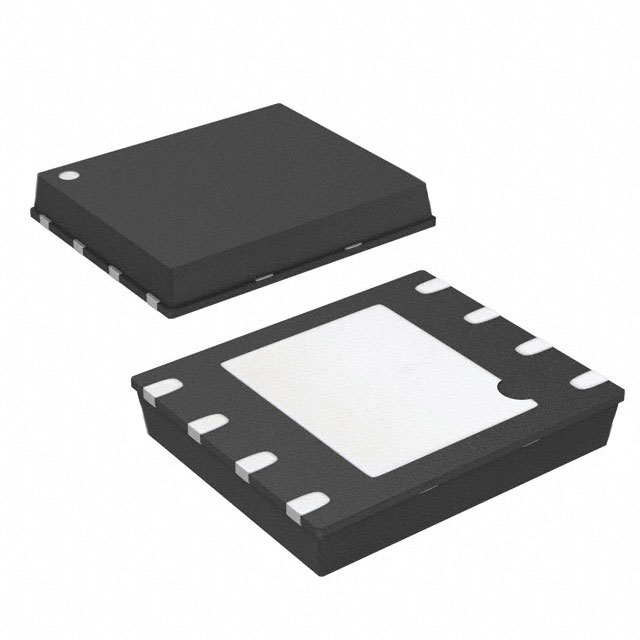
- Package: 8-pin SOIC (Small Outline Integrated Circuit)
- Essence: High-density, low-power, and cost-effective memory solution
- Packaging/Quantity: Tape and Reel, 2500 units per reel
Specifications
- Memory Size: 64 megabits (8 megabytes)
- Interface: Serial Peripheral Interface (SPI)
- Operating Voltage: 2.7V to 3.6V
- Operating Temperature Range: -40°C to +85°C
- Data Retention: More than 20 years
- Program/Erase Cycles: 10,000 minimum
Pin Configuration
The AT45DB641E-MHN2B-T has the following pin configuration:
- Chip Select (/CS)
- Output Enable (/OE)
- Write Protect (/WP)
- Serial Data Input (SI)
- Serial Data Output (SO)
- Serial Clock (SCK)
- Reset (/RESET)
- VCC (Power Supply)
Functional Features
- Dual-interface: Supports both SPI and RapidS serial interface modes
- Page Program Operation: Allows programming of data in page mode
- Continuous Read Mode: Enables sequential reading of data from multiple pages
- Sector Erase Capability: Provides sector-based erase operation
- Deep Power-down Mode: Reduces power consumption when not in use
- Software Protection: Supports software protection of memory sectors
Advantages and Disadvantages
Advantages: - High-density memory for storing large amounts of data - Low power consumption, suitable for battery-powered devices - Fast data transfer rate through the SPI interface - Long data retention period ensures data integrity
Disadvantages: - Limited program/erase cycles may affect the lifespan of the memory - Requires external microcontroller or host device for operation - Relatively small package size limits compatibility with certain systems
Working Principles
The AT45DB641E-MHN2B-T is based on the NOR Flash memory technology. It utilizes a combination of floating-gate transistors and control circuitry to store and retrieve digital data. The memory cells are organized into sectors, pages, and bytes, allowing efficient read and write operations.
During programming, data is written to the memory by applying appropriate voltage levels to the control pins. Erasing of data can be performed at the sector level, ensuring selective removal of information. The memory can be accessed using the SPI interface, enabling easy integration with various microcontrollers and systems.
Detailed Application Field Plans
The AT45DB641E-MHN2B-T is widely used in applications that require non-volatile data storage and retrieval. Some common application fields include:
- Consumer Electronics: Used in digital cameras, portable media players, and gaming consoles for storing firmware, configuration settings, and user data.
- Industrial Automation: Employed in programmable logic controllers (PLCs), data loggers, and industrial control systems for storing critical operational parameters and event logs.
- Automotive Systems: Integrated into automotive infotainment systems, instrument clusters, and electronic control units (ECUs) to store software updates, calibration data, and diagnostic information.
- Medical Devices: Utilized in medical equipment such as patient monitors, infusion pumps, and diagnostic devices for storing patient data, firmware, and system configurations.
Alternative Models
- AT45DB321E-MHN2B-T: 32 megabit (4 megabyte) version of the same series
- AT45DB081E-MHN2B-T: 8 megabit (1 megabyte) version of the same series
- AT45DB641D-MU: Similar capacity and features, but in a different package (48-ball TFBGA)
These alternative models offer similar functionality and can be considered as replacements based on specific requirements.
Word count: 510 words
Sebutkan 10 pertanyaan dan jawaban umum terkait penerapan AT45DB641E-MHN2B-T dalam solusi teknis
Sure! Here are 10 common questions and answers related to the application of AT45DB641E-MHN2B-T in technical solutions:
Q: What is the AT45DB641E-MHN2B-T? A: The AT45DB641E-MHN2B-T is a high-density flash memory device manufactured by Adesto Technologies. It offers 64 megabits (8 megabytes) of storage capacity.
Q: What are the main features of the AT45DB641E-MHN2B-T? A: The key features include a serial interface, dual power supply operation, fast read and write operations, sector-based architecture, and low power consumption.
Q: How can I interface with the AT45DB641E-MHN2B-T? A: The AT45DB641E-MHN2B-T uses a standard SPI (Serial Peripheral Interface) for communication, making it compatible with a wide range of microcontrollers and other devices.
Q: What is the maximum data transfer rate of the AT45DB641E-MHN2B-T? A: The device supports a maximum clock frequency of 85 MHz, allowing for fast data transfer rates during read and write operations.
Q: Can I use the AT45DB641E-MHN2B-T in battery-powered applications? A: Yes, the AT45DB641E-MHN2B-T has low power consumption characteristics, making it suitable for battery-powered devices where energy efficiency is crucial.
Q: Does the AT45DB641E-MHN2B-T support wear-leveling algorithms? A: No, the AT45DB641E-MHN2B-T does not have built-in wear-leveling algorithms. However, you can implement wear-leveling techniques in your software to extend the lifespan of the flash memory.
Q: Can I perform in-system programming on the AT45DB641E-MHN2B-T? A: Yes, the AT45DB641E-MHN2B-T supports in-system programming, allowing you to update the firmware or data stored in the flash memory without removing it from the system.
Q: What is the typical endurance of the AT45DB641E-MHN2B-T? A: The AT45DB641E-MHN2B-T has a typical endurance of 100,000 write cycles per sector, ensuring reliable and long-lasting operation.
Q: Is the AT45DB641E-MHN2B-T suitable for high-temperature environments? A: Yes, the AT45DB641E-MHN2B-T is designed to operate reliably in a wide temperature range, typically from -40°C to +85°C.
Q: Are there any development tools or resources available for the AT45DB641E-MHN2B-T? A: Yes, Adesto Technologies provides documentation, datasheets, application notes, and software libraries to assist developers in integrating the AT45DB641E-MHN2B-T into their technical solutions.
Please note that these answers are general and may vary depending on specific use cases and requirements.