

Lihat spesifikasi untuk detail produk.
S-80956CLNB-G7ST2G
Product Overview
Category
S-80956CLNB-G7ST2G belongs to the category of integrated circuits (ICs).
Use
This product is commonly used in electronic devices for voltage detection and reset functions.
Characteristics
- Voltage detection range: 1.6V to 5.0V
- Low supply current: 1.0µA (typ.)
- Small package size: SOT-23-5
- Built-in delay circuit for stable reset operation
- Wide operating temperature range: -40°C to +85°C
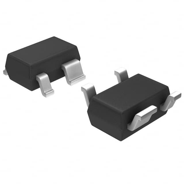
Package
S-80956CLNB-G7ST2G is packaged in a small outline transistor (SOT) package, specifically SOT-23-5.
Essence
The essence of this product lies in its ability to accurately detect voltage levels and provide reliable reset functionality in electronic devices.
Packaging/Quantity
This product is typically available in tape and reel packaging, with a quantity of 3000 units per reel.
Specifications
- Supply voltage range: 1.6V to 5.5V
- Reset threshold voltage options: 2.3V, 2.8V, 3.1V, 4.0V
- Output type: Active low
- Quiescent current: 1.0µA (typ.)
- Reset output current: 10mA (max.)
- Operating temperature range: -40°C to +85°C
Detailed Pin Configuration
The S-80956CLNB-G7ST2G IC has the following pin configuration:
- VDD (Supply Voltage)
- GND (Ground)
- MR (Manual Reset)
- RESET (Reset Output)
- VOUT (Voltage Detection Output)
Functional Features
- Accurate voltage detection within the specified range
- Built-in delay circuit ensures stable reset operation
- Manual reset function for additional control
- Active low reset output signal
Advantages and Disadvantages
Advantages
- Wide voltage detection range allows for versatile applications
- Low supply current minimizes power consumption
- Small package size enables space-saving designs
- Reliable reset functionality enhances system stability
Disadvantages
- Limited reset threshold voltage options may not suit all requirements
- Reset output current limitation may restrict certain applications
Working Principles
The S-80956CLNB-G7ST2G operates by continuously monitoring the input voltage level. When the voltage falls below the preset threshold, the reset output is activated, indicating a low-voltage condition. The built-in delay circuit ensures that the reset signal remains stable during power-up or transient voltage fluctuations.
Detailed Application Field Plans
The S-80956CLNB-G7ST2G finds extensive use in various electronic devices, including but not limited to: - Microcontrollers - Power management systems - Battery-powered devices - Industrial automation equipment - Consumer electronics
Detailed and Complete Alternative Models
- S-80930CNMC-G8XT2G
- S-80942CNMC-G8XT2G
- S-80946CNMC-G8XT2G
- S-80950CNMC-G8XT2G
- S-80960CNMC-G8XT2G
These alternative models offer similar voltage detection and reset functionalities, catering to different voltage threshold requirements.
In conclusion, the S-80956CLNB-G7ST2G integrated circuit provides accurate voltage detection and reliable reset functionality in electronic devices. Its wide operating temperature range, low supply current, and small package size make it suitable for various applications. However, the limited reset threshold voltage options and reset output current limitation should be considered when selecting this product.
Sebutkan 10 pertanyaan dan jawaban umum terkait penerapan S-80956CLNB-G7ST2G dalam solusi teknis
Sure! Here are 10 common questions and answers related to the application of S-80956CLNB-G7ST2G in technical solutions:
1. What is the S-80956CLNB-G7ST2G? - The S-80956CLNB-G7ST2G is a voltage detector IC (integrated circuit) manufactured by a specific company.
2. What is the purpose of the S-80956CLNB-G7ST2G? - The purpose of this IC is to monitor the voltage level of a power supply and provide an output signal when the voltage falls below a certain threshold.
3. What are the typical applications of the S-80956CLNB-G7ST2G? - This IC is commonly used in various technical solutions such as battery-powered devices, power management systems, and low-power microcontroller circuits.
4. What is the operating voltage range of the S-80956CLNB-G7ST2G? - The operating voltage range of this IC is typically between 1.6V and 6.0V.
5. What is the output type of the S-80956CLNB-G7ST2G? - The output of this IC is an open-drain N-channel transistor.
6. What is the quiescent current consumption of the S-80956CLNB-G7ST2G? - The quiescent current consumption of this IC is typically around 1.0µA.
7. What is the hysteresis voltage of the S-80956CLNB-G7ST2G? - The hysteresis voltage of this IC is typically around 50mV.
8. Can the S-80956CLNB-G7ST2G be used for overvoltage detection? - No, this IC is specifically designed for undervoltage detection and does not support overvoltage detection.
9. What is the temperature range of operation for the S-80956CLNB-G7ST2G? - The temperature range of operation for this IC is typically between -40°C and +85°C.
10. Is the S-80956CLNB-G7ST2G RoHS compliant? - Yes, this IC is RoHS (Restriction of Hazardous Substances) compliant, ensuring it meets certain environmental standards.
Please note that the answers provided here are general and may vary depending on the specific datasheet and manufacturer's specifications for the S-80956CLNB-G7ST2G.