

Lihat spesifikasi untuk detail produk.
S-80924CNNB-G8UT2G
Product Overview
Category
S-80924CNNB-G8UT2G belongs to the category of integrated circuits (ICs).
Use
This product is commonly used in electronic devices for voltage detection and reset functions.
Characteristics
- Voltage detection range: 1.0V to 5.0V
- Low supply current: 1.0µA (typical)
- High accuracy: ±1.0%
- Built-in delay circuit
- Small package size: SOT-23-5
Package
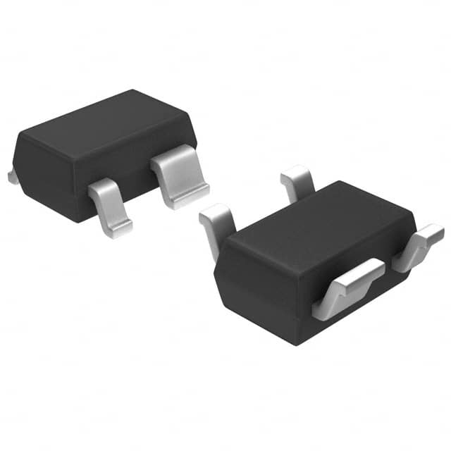
The S-80924CNNB-G8UT2G is packaged in a small outline transistor (SOT) package, specifically SOT-23-5. This package provides compactness and ease of integration into various electronic devices.
Essence
The essence of S-80924CNNB-G8UT2G lies in its ability to accurately detect voltage levels within a specified range and provide a reset signal when necessary. This feature ensures proper functioning and reliability of electronic devices.
Packaging/Quantity
The S-80924CNNB-G8UT2G is typically available in reels containing 3000 units per reel.
Specifications
- Supply voltage range: 1.6V to 5.5V
- Operating temperature range: -40°C to +85°C
- Output type: Active low
- Reset threshold voltage options: 1.0V, 1.1V, 1.2V, 1.3V, 1.4V, 1.5V, 1.6V, 1.7V, 1.8V, 1.9V, 2.0V, 2.1V, 2.2V, 2.3V, 2.4V, 2.5V, 2.6V, 2.7V, 2.8V, 2.9V, 3.0V, 3.1V, 3.2V, 3.3V, 3.4V, 3.5V, 3.6V, 3.7V, 3.8V, 3.9V, 4.0V, 4.1V, 4.2V, 4.3V, 4.4V, 4.5V, 4.6V, 4.7V, 4.8V, 4.9V, 5.0V
Detailed Pin Configuration
The S-80924CNNB-G8UT2G has a total of five pins:
- VDD: Supply voltage input
- GND: Ground reference
- RESET: Active low reset output
- MR: Manual reset input (optional)
- VOUT: Voltage detection output
Functional Features
Voltage Detection
The S-80924CNNB-G8UT2G is designed to accurately detect the voltage level applied to its input pin. It compares this voltage with the preset threshold voltage and generates a reset signal when the voltage falls below the threshold.
Reset Output
When the voltage drops below the threshold, the S-80924CNNB-G8UT2G provides an active low reset signal through its RESET pin. This signal can be used to initiate system resets or trigger specific actions in electronic devices.
Built-in Delay Circuit
To prevent false triggering due to momentary voltage fluctuations, the S-80924CNNB-G8UT2G incorporates a built-in delay circuit. This delay ensures that the reset signal is stable and reliable, even in the presence of temporary voltage variations.
Advantages and Disadvantages
Advantages
- Wide operating voltage range
- High accuracy voltage detection
- Low supply current consumption
- Compact package size for space-constrained applications
- Built-in delay circuit for reliable reset signals
Disadvantages
- Limited number of available threshold voltage options
- Active low reset output may not be suitable for all applications
Working Principles
The S-80924CNNB-G8UT2G operates based on a voltage comparator principle. It compares the input voltage with the preset threshold voltage and generates a corresponding reset signal when the input voltage falls below the threshold. The built-in delay circuit ensures stable and reliable reset signals, preventing false triggering due to momentary voltage fluctuations.
Detailed Application Field Plans
The S-80924CNNB-G8UT2G finds application in various electronic devices where accurate voltage detection and reliable reset functionality are crucial. Some potential application fields include:
- Microcontrollers and microprocessors
- Power management systems
- Battery-powered devices
- Industrial automation equipment
- Consumer electronics
Detailed and
Sebutkan 10 pertanyaan dan jawaban umum terkait penerapan S-80924CNNB-G8UT2G dalam solusi teknis
Sure! Here are 10 common questions and answers related to the application of S-80924CNNB-G8UT2G in technical solutions:
1. What is the S-80924CNNB-G8UT2G? - The S-80924CNNB-G8UT2G is a voltage detector IC (integrated circuit) manufactured by a specific company.
2. What is the purpose of the S-80924CNNB-G8UT2G? - The purpose of this IC is to monitor the voltage level of a power supply and provide an output signal when the voltage falls below a certain threshold.
3. What are the typical applications of the S-80924CNNB-G8UT2G? - This IC is commonly used in various technical solutions such as battery-powered devices, power management systems, and low-power microcontroller circuits.
4. What is the operating voltage range of the S-80924CNNB-G8UT2G? - The operating voltage range of this IC is typically between 1.6V and 6.0V.
5. How accurate is the voltage detection of the S-80924CNNB-G8UT2G? - The voltage detection accuracy of this IC is typically within ±1.0%.
6. What is the output configuration of the S-80924CNNB-G8UT2G? - The output configuration of this IC is an open-drain output, which requires an external pull-up resistor.
7. Can the S-80924CNNB-G8UT2G be used in automotive applications? - Yes, this IC is suitable for automotive applications as it meets the necessary standards and requirements.
8. Does the S-80924CNNB-G8UT2G have any built-in protection features? - Yes, this IC includes built-in protection features such as overcurrent protection and thermal shutdown.
9. What is the package type of the S-80924CNNB-G8UT2G? - The S-80924CNNB-G8UT2G is available in a small surface-mount package called SOT-23-5.
10. Where can I find more information about the S-80924CNNB-G8UT2G? - You can refer to the datasheet provided by the manufacturer for detailed information on the specifications, pin configuration, and application notes of the S-80924CNNB-G8UT2G.
Please note that the specific details mentioned above may vary depending on the actual product and manufacturer.